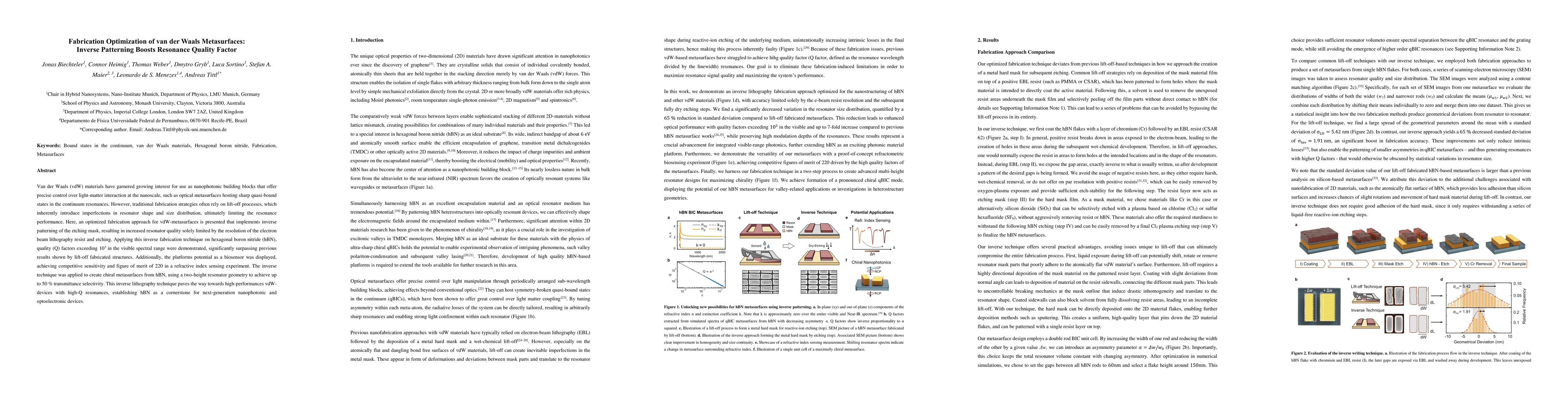
Van der Waals (vdW) materials have garnered growing interest for use as
nanophotonic building blocks that offer precise control over light-matter
interaction at the nanoscale, such as optical metasurfaces hosting sharp
quasi-bound states in the continuum resonances. However, traditional
fabrication strategies often rely on lift-off processes, which inherently
introduce imperfections in resonator shape and size distribution, ultimately
limiting the resonance performance. Here, an optimized fabrication approach for
vdW-metasurfaces is presented that implements inverse patterning of the etching
mask, resulting in increased resonator quality solely limited by the resolution
of the electron beam lithography resist and etching. Applying this inverse
fabrication technique on hexagonal boron nitride (hBN), quality (Q) factors
exceeding $10^3$ in the visible spectral range were demonstrated, significantly
surpassing previous results shown by lift-off fabricated structures.
Additionally, the platforms potential as a biosensor was displayed, achieving
competitive sensitivity and figure of merit of 220 in a refractive index
sensing experiment. The inverse technique was applied to create chiral
metasurfaces from hBN, using a two-height resonator geometry to achieve up to
50 % transmittance selectivity. This inverse lithography technique paves the
way towards high-performances vdW-devices with high-Q resonances, establishing
hBN as a cornerstone for next-generation nanophotonic and optoelectronic
devices.
Discussion 0