Quick Summary:

This paper investigates the Faraday cage angled-etching (FCAE) technique for in-situ device release and isolation in optoelectronic materials, demonstrating its ability to direct etching plasma ions for precise control over etch angle, uniformity, and mask selectivity. Simulation and experimental results elucidate the effects of Faraday cage angle, mesh size, and sample placement, providing guidelines for FCAE process design across various material platforms.

Summary

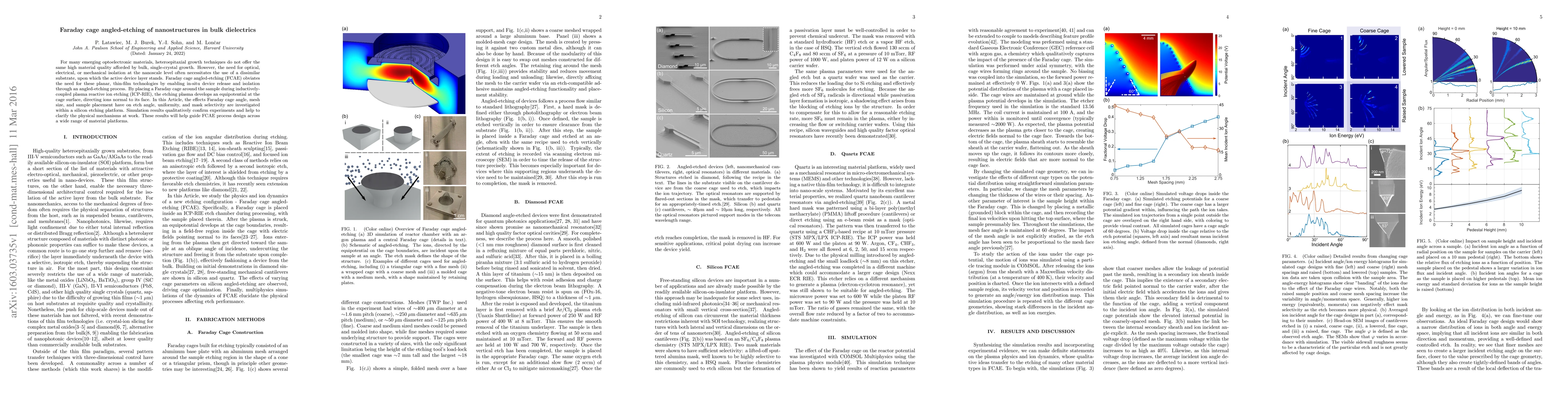
For many emerging optoelectronic materials, heteroepitaxial growth techniques do not offer the same high material quality afforded by bulk, single-crystal growth. However, the need for optical, electrical, or mechanical isolation at the nanoscale level often necessitates the use of a dissimilar substrate, upon which the active device layer stands. Faraday cage angled-etching (FCAE) obviates the need for these planar, thin-film technologies by enabling in-situ device release and isolation through an angled-etching process. By placing a Faraday cage around the sample during inductively-coupled plasma reactive ion etching (ICP-RIE), the etching plasma develops an equipotential at the cage surface, directing ions normal to its face. In this Article, the effects Faraday cage angle, mesh size, and sample placement have on etch angle, uniformity, and mask selectivity are investigated within a silicon etching platform. Simulation results qualitatively confirm experiments and help to clarify the physical mechanisms at work. These results will help guide FCAE process design across a wide range of material platforms.

AI Key Findings

Get AI-generated insights about this paper's methodology, results, and significance.

Paper Details

PDF Preview

Download PDF

Key Terms

device (0.203)
plasma (0.194)
angle (0.185)
help (0.183)
material (0.182)
growth (0.181)
need (0.163)
situ (0.151)
sample (0.149)
placement (0.147)
clarify (0.145)
single crystal (0.143)
nanoscale (0.141)
mask (0.139)
mesh (0.139)
substrate (0.137)
qualitatively (0.136)
guide (0.136)
develops (0.136)
release (0.132)

Citation Network

Current paper (gray), citations (green), references (blue)

Current Paper
Citations
References
Click to view

Similar Papers

No similar papers found for this research.

Title Authors Year Actions
Damage-free sputtering of a transparent conductive oxide using a triode plasma configuration
J. An, Ji-Eun Hong, Sung-In Mo, Yimhyun Jo, Sinho Choi, Tae-Hee Kim, Soong Ju Oh, Kyung Taek Jeong, Hee-eun Song, Joon-Ho Oh, Ka-Hyun Kim
2025
View Paper
Preparation of Silicon Nanopillar Arrays Using Reactive Ion Etching with a Faraday Cage.
Lihui Yu, Qiutong Zhao, Jingquan Guo, Yingjie Fan, Jingjing Zhang, Yilin Zhang, Shujun Ye
2025
View Paper
Interfacial Elemental Analysis of Slanted Edge-Contacted Monolayer MoS2 Transistors via Directionally Angled Etching
Chia-Chun Lin, N. T. Paylaga, Chun-Chieh Yen, Yu-Hsuan Lin, Kuang-Hsu Wang, Kenji Watanabe, T. Taniguchi, Chi-Te Liang, Shao-Yu Chen, Wei-Hua Wang
2025
View Paper
Fabrication of diamond drum resonators via laser engraving and Si wet etching for high precision temperature sensing
Yunchao Du, Zhixin Zhao, Haoran Li, Biao Yan, Duo Liu
2025
View Paper
Wafer-scale integration of freestanding photonic devices with color centers in silicon carbide
S. Majety, Victoria A. Norman, Pranta Saha, Alex H. Rubin, Scott Dhuey, Marina Radulaski
2024
View Paper
CMOS-Compatible Wafer-Level Double-layer Silicon Nanograss through Reactive Ion Etching for Applications in Optics
Lihui Yu, Jingjing Zhang, Shujun Ye, Qiutong Zhao, Jingquan Guo, Yeliang Wang
2024
View Paper
Fabrication of slanted gratings by using glancing angle deposition
Hongwen Wu, Aixi Pan, Chenxu Zhu, Bo Cui
2024
View Paper
Calculation of coupling coefficients for diamond micro-ring resonators
Quankui Yang, Christian Giese, Stefan Hugger
2024
View Paper
Fabrication of Sawfish photonic crystal cavities in bulk diamond
T. Pregnolato, Marco E. Stucki, J. M. Bopp, Maarten H. v. d. Hoeven, Alok Gokhale, Olaf Krüger, Tim Schröder
2023
View Paper
Hybrid integration of ensemble nitrogen-vacancy centers in single-crystal diamond based on pick-flip-and-place transfer printing
Ryota Katsumi, Kosuke Takada, Shun Naruse, Kenta Kawai, Daichi Sato, Takeshi Hizawa, Takashi Yatsui
2023
View Paper
Emerging material platforms for integrated microcavity photonics
Jin Liu, Fang Bo, Lin‐Shen Chang, C. Dong, Xinxiu Ou, Blake Regan, Xiaoqin Shen, Q. Song, B. Yao, Wenfu Zhang, Chang‐Ling Zou, Yun-Feng Xiao
2022
View Paper
Development of hard masks for reactive ion beam angled etching of diamond.
Cleaven Chia, B. Machielse, A. Shams-Ansari, M. Lončar
2022
View Paper
Slanted Nanostructures Capped with SiO2 Nanospheres for Asymmetric Hydrophilicity Inducing Rapid Unidirectional Water Spreading
Lan Thi Phan, Sang Jin Park, M. Moon
2021
View Paper
Progress in semiconductor diamond photodetectors and MEMS sensors
M. Liao
2021
View Paper
Diamond photonic crystal mirror with a partial bandgap by two 2D photonic crystal layers.
Seungwoo Jeon, Kiwon Kwon, Sang-Wook Han, Yong-Su Kim, Young-Wook Cho, Hyang-Tag Lim, Sung Moon, Heedeuk Shin, Hojoong Jung
2020
View Paper
Adjoint-optimized nanoscale light extractor for nitrogen-vacancy centers in diamond
R. Wambold, Zhaoning Yu, Yuzhe Xiao, Benjamin Bachman, G. Jaffe, S. Kolkowitz, J. Choy, M. Eriksson, R. Hamers, M. Kats
2020
View Paper
Development of All-Diamond Scanning Probes Based on Faraday Cage Angled Etching Techniques
C. Giese, P. Quellmalz, P. Knittel
2020
View Paper
Faraday-cage-assisted etching of suspended gallium nitride nanostructures
Geraint P. Gough, A. Sobiesierski, Saleem Shabbir, Stuart N. Thomas, D. Beggs, R. Taylor, A. Bennett
2020
View Paper
Capacitive Silicon Modulator Design With V-Shaped SiO$_{2}$ Gate Waveguide to Optimize $V_{\pi }\times L$ and Bandwidth Trade-Off
D. M. Dourado, G. B. de Farias, Yesica R. R. Bustamante, M. Rocha, J. Carmo
2020
View Paper
Oblique angled plasma etching for 3D silicon structures with wiggling geometries
Bingdong Chang
2019
View Paper
Polishing, preparation and patterning of diamond for device applications
Marie-Laure Hicks, A. Pakpour-Tabrizi, R. Jackman
2019
View Paper
Ripple formation on Si surfaces during plasma etching in Cl2
Nobuya Nakazaki, H. Matsumoto, S. Sonobe, Takumi Hatsuse, H. Tsuda, Y. Takao, K. Eriguchi, K. Ono
2018
View Paper
Mechanical and optical nanodevices in single-crystal quartz
Young-Ik Sohn, Rachel Miller, V. Venkataraman, Marko Lonvcar
2017
View Paper
Strongly Cavity-Enhanced Spontaneous Emission from Silicon-Vacancy Centers in Diamond.
J. Zhang, Shuo Sun, M. Burek, C. Dory, Yan-Kai Tzeng, K. Fischer, Yousif A. Kelaita, K. Lagoudakis, M. Radulaski, Z. Shen, N. Melosh, S. Chu, M. Lončar, J. Vučković
2017
View Paper
Tipping solutions: emerging 3D nano-fabrication/ -imaging technologies
G. Seniutinas, A. Balčytis, I. Reklaitis, Feng Chen, Jeffrey A. Davis, C. David, S. Juodkazis
2017
View Paper
Angled etching of Si by ClF3–Ar gas cluster injection
T. Seki, Hiroki Yamamoto, T. Kozawa, T. Shojo, K. Koike, T. Aoki, J. Matsuo
2017
View Paper
Freestanding nanostructures via reactive ion beam angled etching
H. Atikian, P. Latawiec, M. Burek, Young-Ik Sohn, S. Meesala, N. Gravel, A. Kouki, M. Lončar
2017
View Paper
Fabrication of a Si lever structure made by double-angled etching with reactive gas cluster injection
T. Seki, Hiroki Yamamoto, T. Kozawa, K. Koike, T. Aoki, J. Matsuo
2017
View Paper
A fiber-coupled diamond quantum nanophotonic interface
M. Burek, Charles Meuwly, R. Evans, M. Bhaskar, A. Sipahigil, S. Meesala, D. Sukachev, C. Nguyen, J. Pacheco, E. Bielejec, M. Lukin, Marko Lonvcar
2016
View Paper
Diamond optomechanical crystals
M. Burek, Justin D. Cohen, S. Meenehan, N. El-Sawah, Cleaven Chia, Thibaud Ruelle, S. Meesala, Jake Rochman, H. Atikian, M. Markham, D. Twitchen, M. Lukin, O. Painter, Marko Lonvcar
2015
View Paper
Waveguide-loaded silica fibers for coupling to high-index micro-resonators
P. Latawiec, M. Burek, V. Venkataraman, Marko Lonvcar
2015
View Paper
Metasurface mirrors based on homogeneous materials for high-power lasers
Runxue Leng, Z. Zhu, Jianfa Zhang
2024
View Paper
Diamond optomechanical crystals : supplementary material
M. Burek, Justin D. Cohen, S. Meenehan, N. El-Sawah, Cleaven Chia, Thibaud Ruelle, S. Meesala, Jake Rochman, H. Atikian, M. Markham, D. Twitchen, M. Lukin, O. Painter
2016
View Paper

Comments (0)

This website uses cookies to ensure you get the best experience. Learn more