Fast transient charge trapping in salt-aided CVD synthesized monolayer MoS2 field-effect transistor
Publication
Metrics
AI Quick Summary
This paper investigates fast transient charge trapping in CVD-synthesized monolayer MoS2 field-effect transistors, achieving a 100% increase in field-effect mobility and hysteresis-free transfer characteristics through pulse methodologies. Density functional theory analyses reveal Schottky barrier and metal-induced gap state effects, highlighting potential for advanced memory, logic, and sensor applications.
Paper Preview
Abstract
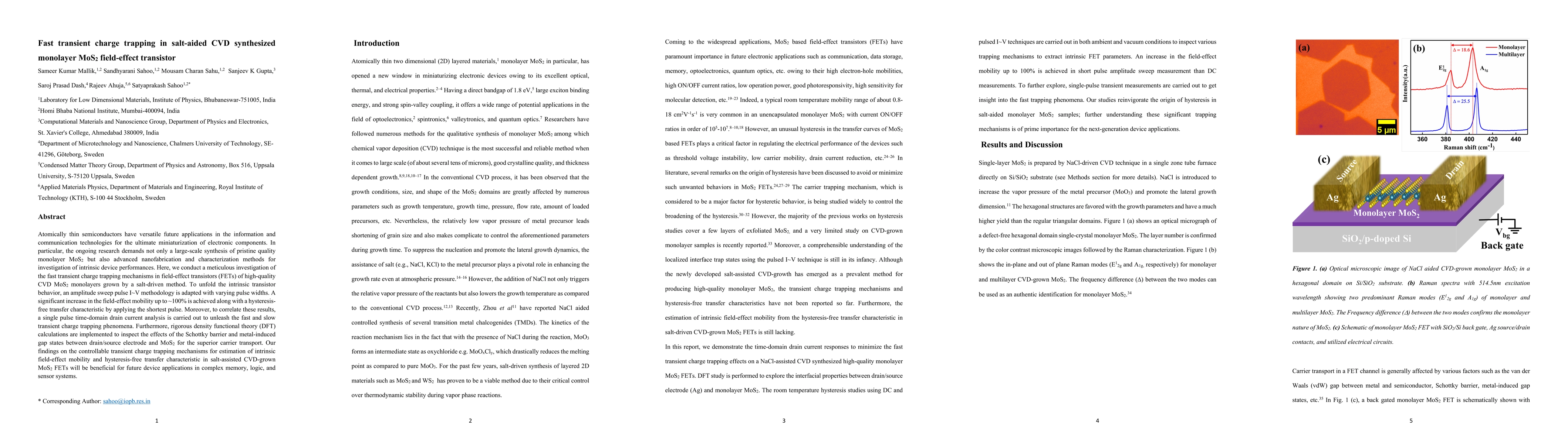
Atomically thin semiconductors have versatile future applications in the information and communication technologies for the ultimate miniaturization of electronic components. In particular, the ongoing research demands not only a large-scale synthesis of pristine quality monolayer MoS2 but also advanced nanofabrication and characterization methods for investigation of intrinsic device performances. Here, we conduct a meticulous investigation of the fast transient charge trapping mechanisms in field-effect transistors (FETs) of high-quality CVD MoS2 monolayers grown by a salt-driven method. To unfold the intrinsic transistor behavior, an amplitude sweep pulse I~V methodology is adapted with varying pulse widths. A significant increase in the field-effect mobility up to ~100% is achieved along with a hysteresis-free transfer characteristic by applying the shortest pulse. Moreover, to correlate these results, a single pulse time-domain drain current analysis is carried out to unleash the fast and slow transient charge trapping phenomena. Furthermore, rigorous density functional theory (DFT) calculations are implemented to inspect the effects of the Schottky barrier and metal-induced gap states between drain/source electrode and MoS2 for the superior carrier transport. Our findings on the controllable transient charge trapping mechanisms for estimation of intrinsic field-effect mobility and hysteresis-free transfer characteristic in salt-assisted CVD-grown MoS2 FETs will be beneficial for future device applications in complex memory, logic, and sensor systems.
AI Key Findings
Get AI-generated insights about this paper's methodology, results, significance, and more — seven facets brought into focus.
Impact
Paper Details
Authors
PDF Preview
Key Terms
Citation Network
Current paper (gray), citations (green), references (blue)
Display is limited for performance on very large graphs.
Discussion 0