Authors
Summary
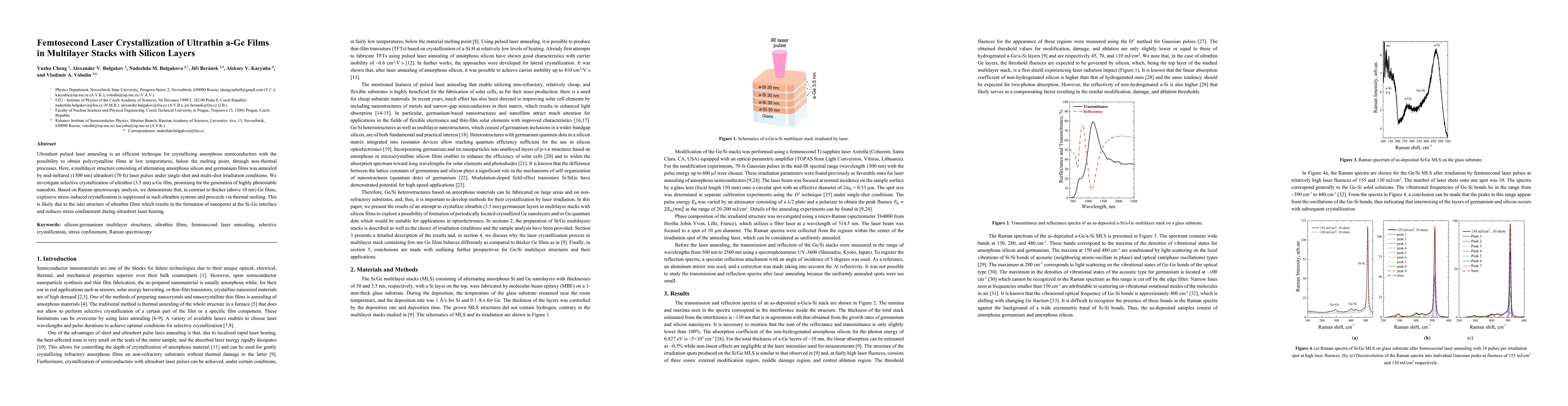
Ultrashort pulsed laser annealing is an efficient technique for crystallizing amorphous semiconductors with the possibility to obtain polycrystalline films at low temperatures, below the melting point, through non-thermal processes. Here, a multilayer structure consisting of alternating amorphous silicon and germanium films was annealed by mid-infrared (1500 nm) ultrashort (70 fs) laser pulses under single-shot and multi-shot irradiation conditions. We investigate selective crystallization of ultrathin (3.5 nm) a-Ge film, promising for the generation of highly photostable nanodots. Based on Raman spectroscopy analysis, we demonstrate that, in contrast to thicker (above 10 nm) Ge films, explosive stress-induced crystallization is suppressed in such ultrathin systems and proceeds via thermal melting. This is likely due to the islet structure of ultrathin films which results in the formation of nanopores at the Si-Ge interface and reduces stress confinement during ultrashort laser heating.
AI Key Findings
Generated Oct 01, 2025
Methodology
The study employs ultrafast laser processing techniques to selectively crystallize amorphous Ge/Si multilayer structures, utilizing femtosecond and picosecond infrared lasers to induce non-thermal crystallization without melting.
Key Results
- Successful single-shot crystallization of Ge/Si multilayers with high spatial resolution and minimal thermal damage
- Observation of non-thermal crystallization mechanisms that bypass conventional melting processes
- Demonstration of controlled nanostructure formation with precise dimensional control over the resulting crystalline phases
Significance
This research advances semiconductor nanofabrication by enabling precise, damage-free crystallization of complex multilayer structures, which could significantly impact optoelectronics, photovoltaics, and integrated photonics.
Technical Contribution
The work introduces a novel non-thermal laser crystallization approach that enables precise control over nanoscale semiconductor structure formation without conventional thermal melting processes.
Novelty
This study presents the first demonstration of single-shot, ultrafast laser-induced crystallization of Ge/Si multilayers with simultaneous control over both crystalline phase composition and nanostructure morphology.
Limitations
- The technique may have limited applicability to certain material systems with different thermal properties
- Requires sophisticated laser systems and precise control parameters that may be challenging for industrial implementation
Future Work
- Exploring the technique's applicability to other semiconductor heterostructures beyond Ge/Si
- Developing scalable manufacturing processes for industrial applications
- Investigating the long-term stability and performance of laser-crystallized nanostructures
Paper Details
PDF Preview
Similar Papers
Found 4 papersPhotoluminescence of Femtosecond Laser-irradiated Silicon Carbide
D. Herrmann, S. Weber, Y. Abdedou et al.
Comments (0)