Fermi-level depinning in metal-2D multilayered semiconductor junctions
Publication
Metrics
AI Quick Summary
This paper uses first-principles calculations to demonstrate that the Fermi-level pinning factor in metal-2D multilayered semiconductor junctions (MmSJ) is strongly influenced by the layer-number of few-layer 2D semiconductors. The extended FLP theory reveals weakened overall pinning and depinning between van der Waals layers, leading to favorable p-type contacts and type II band alignments, which are crucial for CMOS and optoelectronic devices.
Paper Preview
Abstract
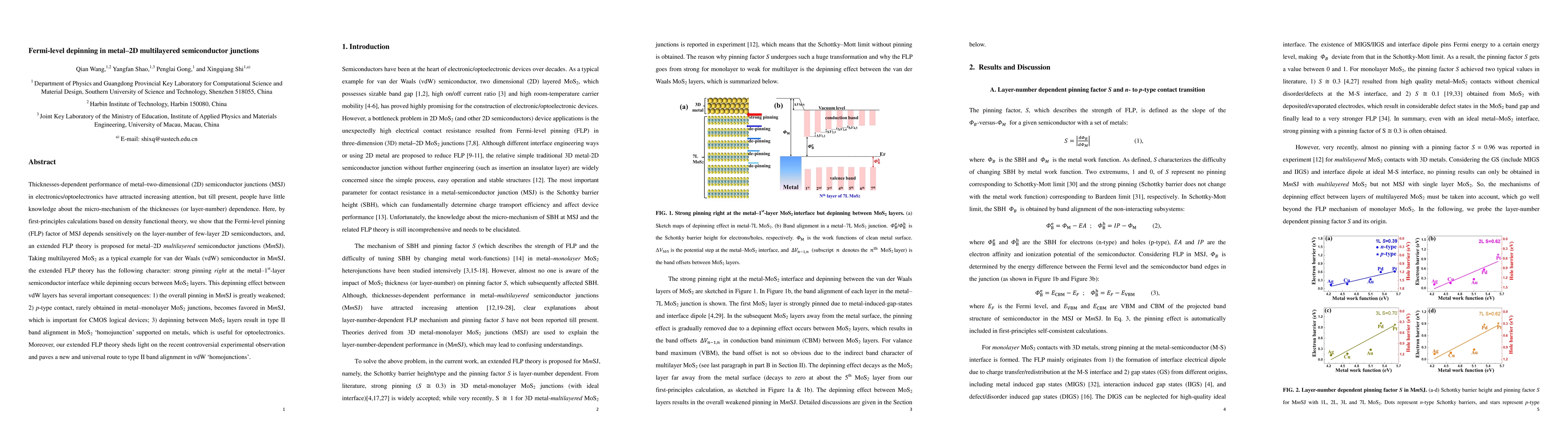
Thicknesses-dependent performance of metal-two-dimensional (2D) semiconductor junctions (MSJ) in electronics/optoelectronics have attracted increasing attention, but till present, people have little knowledge about the micro-mechanism of the thicknesses (or layer-number) dependence. Here, by first-principles calculations based on density functional theory, we show that the Fermi-level pinning (FLP) factor of MSJ depends sensitively on the layer-number of few-layer 2D semiconductors, and, an extended FLP theory is proposed for metal-2D multilayered semiconductor junctions (MmSJ). Taking multilayered MoS2 as a typical example for van der Waals (vdW) semiconductor in MmSJ, the extended FLP theory has the following character: strong pinning right at the metal-1st-layer semiconductor interface while depinning occurs between MoS2 layers. This depinning effect between vdW layers has several important consequences: 1) the overall pinning in MmSJ is greatly weakened; 2) p-type contact, rarely obtained in metal-monolayer MoS2 junctions, becomes favored in MmSJ, which is important for CMOS logical devices; 3) depinning between MoS2 layers result in type II band alignment in MoS2 'homojunction' supported on metals, which is useful for optoelectronics. Moreover, our extended FLP theory sheds light on the recent controversial experimental observation and paves a new and universal route to type II band alignment in vdW 'homojunctions'.
AI Key Findings
Get AI-generated insights about this paper's methodology, results, significance, and more — seven facets brought into focus.
Discussion 0