Ferroelectric Domain Patterning Controlled Schottky Junction State in Monolayer MoS$_2$
Publication
Metrics
AI Quick Summary
This work presents a new route for programmable functionalities in van der Waals materials and sheds light on performance limiting factors in hybrid systems.
Paper Preview
Abstract
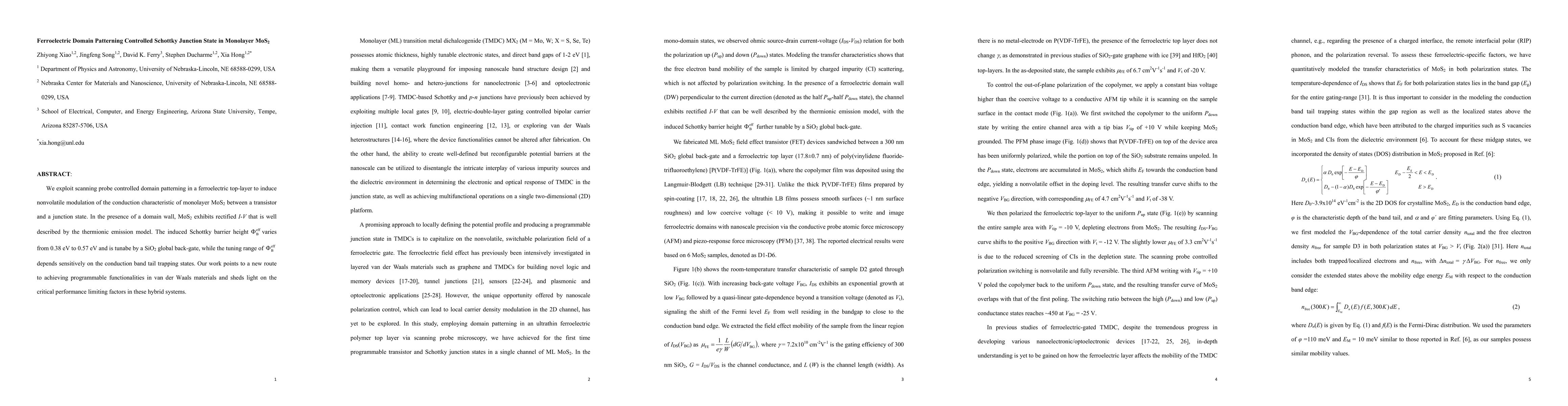
We exploit scanning probe controlled domain patterning in a ferroelectric top layer to induce nonvolatile modulation of the conduction characteristic of monolayer MoS$_2$ between a transistor and a junction state. In the presence of a domain wall, MoS$_2$ exhibits rectified I-V that is well described by the thermionic emission model. The induced Schottky barrier height varies from 0.38 eV to 0.57 eV and is tunabe by a SiO$_2$ global back-gate, while the tuning range of depends sensitively on the conduction band tail trapping states. Our work points to a new route to achieving programmable functionalities in van der Waals materials and sheds light on the critical performance limiting factors in these hybrid systems.
AI Key Findings
Get AI-generated insights about this paper's methodology, results, significance, and more — seven facets brought into focus.
Impact
Paper Details
PDF Preview
Key Terms
Citation Network
Current paper (gray), citations (green), references (blue)
Display is limited for performance on very large graphs.
Discussion 0