Publication
Metrics
AI Quick Summary
This paper investigates how ferroelectric domain structures influence charge modulation in various semiconductors, revealing a complex, nonlinear relationship between domain period, dielectric layer thickness, and semiconductor screening radius. Analytical results provide insights into AFM mapping of ferroelectric surfaces and potential conductivity control in ultra-thin semiconductor layers.
Paper Preview
Abstract
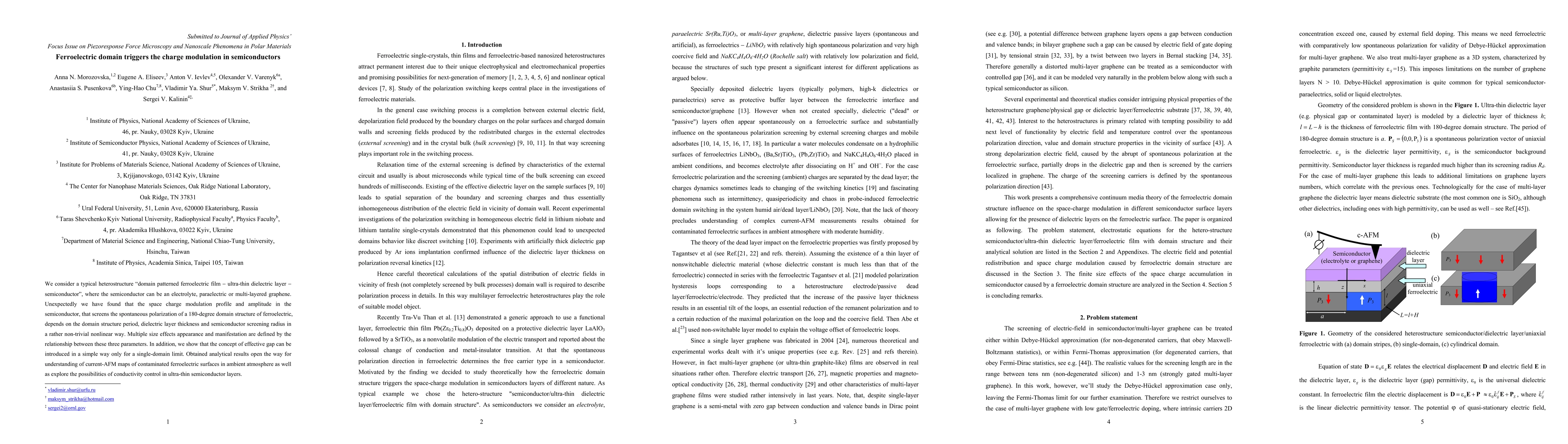
We consider a typical heterostructure domain patterned ferroelectric film/ultra thin dielectric layer/ semiconductor, where the semiconductor can be an electrolyte, paraelectric or multi layered graphene. Unexpectedly we have found that the space charge modulation profile and amplitude in the semiconductor, that screens the spontaneous polarization of a 180-degree domain structure of ferroelectric, depends on the domain structure period, dielectric layer thickness and semiconductor screening radius in a rather non-trivial nonlinear way. Multiple size effects appearance and manifestation are defined by the relationship between these three parameters. In addition, we show that the concept of effective gap can be introduced in a simple way only for a single domain limit. Obtained analytical results open the way for understanding of current AFM maps of contaminated ferroelectric surfaces in ambient atmosphere as well as explore the possibilities of conductivity control in ultra-thin semiconductor layers.
AI Key Findings
Get AI-generated insights about this paper's methodology, results, significance, and more — seven facets brought into focus.
Impact
Paper Details
PDF Preview
Key Terms
Citation Network
Current paper (gray), citations (green), references (blue)
Display is limited for performance on very large graphs.
Discussion 0