Publication
Metrics
AI Quick Summary
This paper investigates n-type Metal Oxide Semiconductor Single Electron Transistors (MOSSETs) fabricated using CMOS technology within a pre-industrial FDSOI framework, achieving a channel size of 20 × 20 nm². The study resolves the Coulomb blockade stability at 4.2 K, revealing large addition energies, and employs CS-DFT for modeling electron confinement, highlighting the potential of CMOS for nanoelectronics and quantum devices.
Paper Preview
Abstract
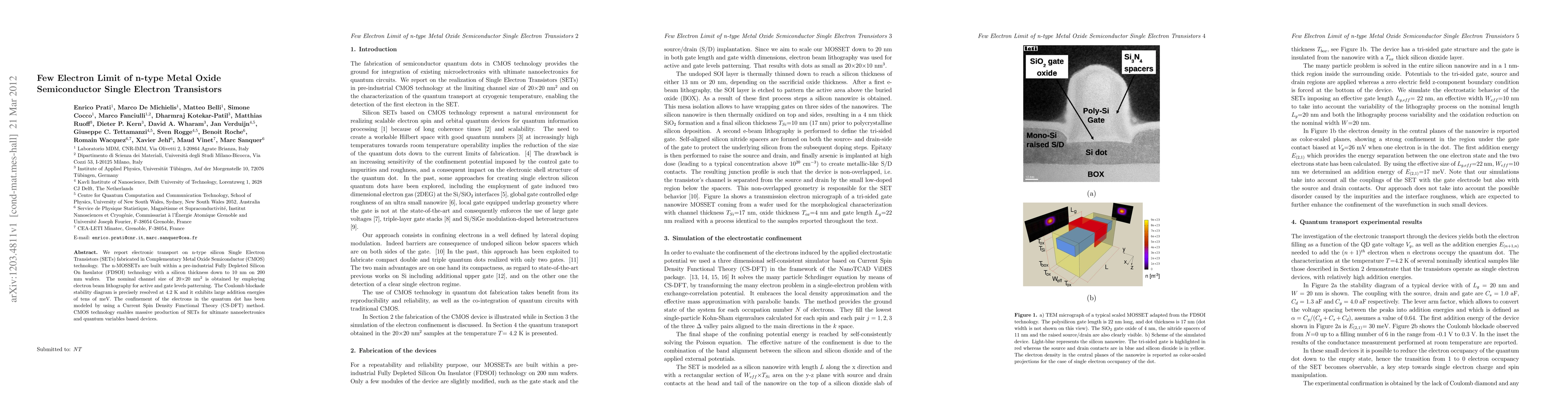
We report electronic transport on n-type silicon Single Electron Transistors (SETs) fabricated in Complementary Metal Oxide Semiconductor (CMOS) technology. The n-MOSSETs are built within a pre-industrial Fully Depleted Silicon On Insulator (FDSOI) technology with a silicon thickness down to 10 nm on 200 mm wafers. The nominal channel size of 20 $\times$ 20 nm$^{2}$ is obtained by employing electron beam lithography for active and gate levels patterning. The Coulomb blockade stability diagram is precisely resolved at 4.2 K and it exhibits large addition energies of tens of meV. The confinement of the electrons in the quantum dot has been modeled by using a Current Spin Density Functional Theory (CS-DFT) method. CMOS technology enables massive production of SETs for ultimate nanoelectronics and quantum variables based devices.
AI Key Findings
Get AI-generated insights about this paper's methodology, results, significance, and more — seven facets brought into focus.
Impact
Paper Details
PDF Preview
Key Terms
Citation Network
Current paper (gray), citations (green), references (blue)
Display is limited for performance on very large graphs.
Discussion 0