Publication
Metrics
AI Quick Summary
Researchers developed a metallic resonant surface that enhances confined electric fields using plasmon-induced resonance, achieving photocurrents 3 orders of magnitude greater than traditional devices.
Paper Preview
Abstract
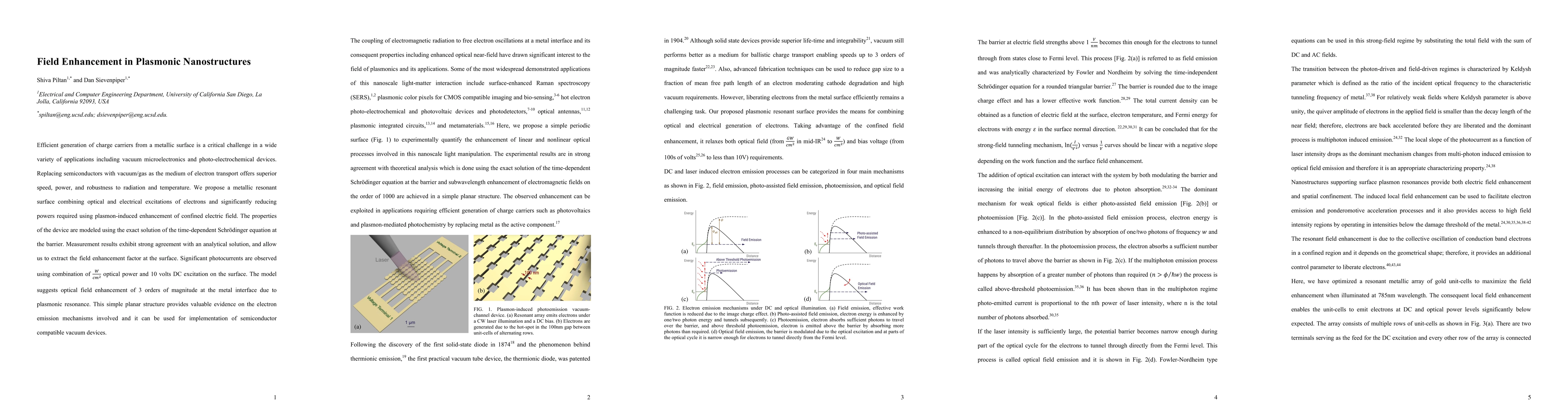
Efficient generation of charge carriers from a metallic surface is a critical challenge in a wide variety of applications including vacuum microelectronics and photo-electrochemical devices. Replacing semiconductors with vacuum/gas as the medium of electron transport offers superior speed, power, and robustness to radiation and temperature. We propose a metallic resonant surface combining optical and electrical excitations of electrons and significantly reducing powers required using plasmon-induced enhancement of confined electric field. The properties of the device are modeled using the exact solution of the time-dependent Schr\"odinger equation at the barrier. Measurement results exhibit strong agreement with an analytical solution, and allow us to extract the field enhancement factor at the surface. Significant photocurrents are observed using combination of W/cm^2 optical power and 10 volts DC excitation on the surface. The model suggests optical field enhancement of 3 orders of magnitude at the metal interface due to plasmonic resonance. This simple planar structure provides valuable evidence on the electron emission mechanisms involved and it can be used for implementation of semiconductor compatible vacuum devices.
AI Key Findings
Get AI-generated insights about this paper's methodology, results, significance, and more — seven facets brought into focus.
Impact
Paper Details
PDF Preview
Key Terms
Citation Network
Current paper (gray), citations (green), references (blue)
Display is limited for performance on very large graphs.
Discussion 0