First principles feasibility assessment of a topological insulator at the InAs/GaSb interface
Publication
Metrics
AI Quick Summary
This study uses first principles simulations to assess the feasibility of a topological insulator phase at the InAs/GaSb interface, comparing it to the HgTe/CdTe interface. While an inverted gap is achievable in InAs/GaSb with an external electric field, the required conditions may be difficult to realize experimentally.
Paper Preview
Abstract
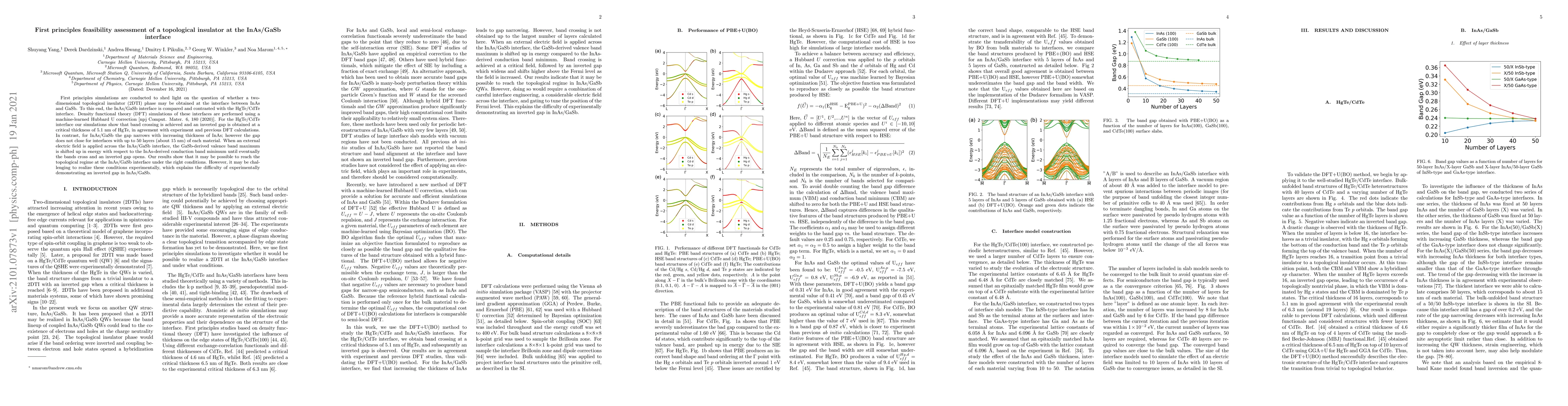
First principles simulations are conducted to shed light on the question of whether a two-dimensional topological insulator (2DTI) phase may be obtained at the interface between InAs and GaSb. To this end, the InAs/GaSb interface is compared and contrasted with the HgTe/CdTe interface. Density functional theory (DFT) simulations of these interfaces are performed using a machine-learned Hubbard U correction [npj Comput. Mater. 6, 180 (2020)]. For the HgTe/CdTe interface our simulations show that band crossing is achieved and an inverted gap is obtained at a critical thickness of 5.1 nm of HgTe, in agreement with experiment and previous DFT calculations. In contrast, for InAs/GaSb the gap narrows with increasing thickness of InAs; however the gap does not close for interfaces with up to 50 layers (about 15 nm) of each material. When an external electric field is applied across the InAs/GaSb interface, the GaSb-derived valence band maximum is shifted up in energy with respect to the InAs-derived conduction band minimum until eventually the bands cross and an inverted gap opens. Our results show that it may be possible to reach the topological regime at the InAs/GaSb interface under the right conditions. However, it may be challenging to realize these conditions experimentally, which explains the difficulty of experimentally demonstrating an inverted gap in InAs/GaSb.
AI Key Findings
Get AI-generated insights about this paper's methodology, results, significance, and more — seven facets brought into focus.
Impact
Paper Details
Authors
PDF Preview
Key Terms
Citation Network
Current paper (gray), citations (green), references (blue)
Display is limited for performance on very large graphs.
Discussion 0