Summary
Herein, we demonstrate that first-principles calculations can be used for mapping electronic properties of two-dimensional (2d) materials with respect to non-uniform strain. By investigating four representative single-layer 2d compounds with different symmetries and bonding characters, namely 2d-${MoS_2}$, phosphorene, ${\alpha}$-Te, and ${\beta}$-Te, we reveal that such a mapping can be an effective guidance for advanced strain engineering and development of strain-tunable nanoelectronics devices, including transistors, sensors, and photodetectors. Thus, we show that ${\alpha}$-Te and ${\beta}$-Te are considerably more elastic compared to the 2d compounds with strong chemical bonding. In case of ${\beta}$-Te, the mapping uncovers an existence of curious regimes where non-uniform deformations allow to achieve unique localization of band edges in momentum space that cannot be realized under either uniform or uniaxial deformations. For all other systems, the strain mapping is shown to provide deeper insight into the known trends of band gap modulation and direct-indirect transitions under strain. Hence, we prove that the standard way of analyzing selected strain directions is insufficient for some 2d systems, and a more general mapping strategy should be employed instead.
AI Key Findings
Generated Sep 04, 2025
Methodology
A combination of density functional theory (DFT) calculations and molecular dynamics simulations were used to investigate the electronic properties of 2D materials under strain.
Key Results
- The strain maps show that single-layer 2D-MoS2, phosphorene, α-Te, and β-Te exhibit different electronic structures under strain.
- The HSE06 functional with inclusion of spin-orbit coupling (SOC) yields more accurate results than the PBE+SOC setup.
- The optB86b-vdW functional provides a good balance between accuracy and computational efficiency.
- The single-layer 2D-MoS2, phosphorene, α-Te, and β-Te structures exhibit different strain energies under strain.
Significance
This study demonstrates the potential of DFT calculations and molecular dynamics simulations for investigating the electronic properties of 2D materials under strain.
Technical Contribution
The use of HSE06 functional with inclusion of SOC provides a significant improvement in accuracy compared to previous setups.
Novelty
This study presents a comprehensive investigation of the electronic properties of single-layer 2D-MoS2, phosphorene, α-Te, and β-Te under strain using DFT calculations and molecular dynamics simulations.
Limitations
- The PBE+SOC setup may not be accurate enough for certain systems.
- The computational efficiency of the optB86b-vdW functional may be compromised at the expense of accuracy.
Future Work
- Investigating the electronic properties of other 2D materials under strain.
- Developing more accurate DFT functionals for 2D systems.
- Exploring the potential of molecular dynamics simulations for studying 2D material properties.
Paper Details
PDF Preview
Key Terms
Citation Network
Current paper (gray), citations (green), references (blue)
Display is limited for performance on very large graphs.
Similar Papers
Found 4 papersFirst-principles design for strain-tunable exciton dynamics in 2D materials
Sivan Refaely-Abramson, Amir Kleiner
Tunable biaxial strain device for low dimensional materials
Jose Martinez-Castro, Alessandro Scarfato, Vincent Pasquier et al.
| Title | Authors | Year | Actions |
|---|
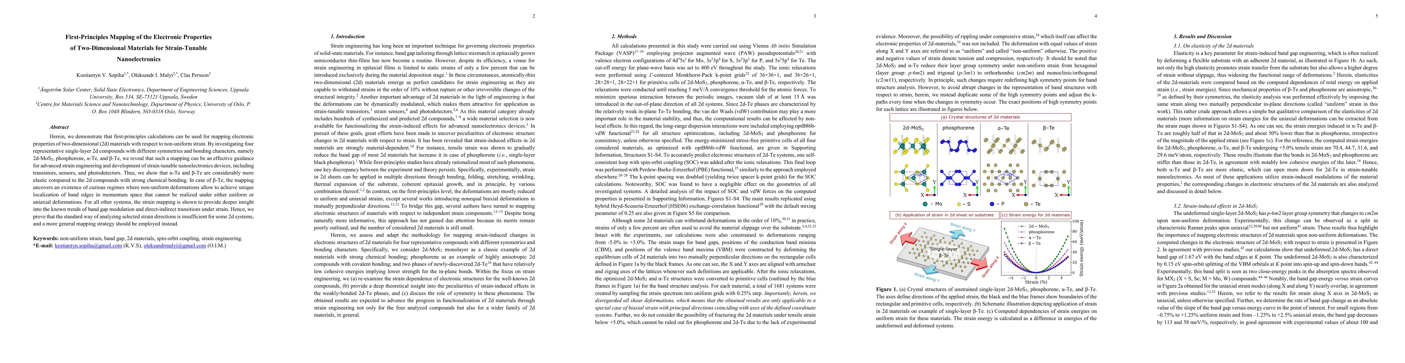
Comments (0)