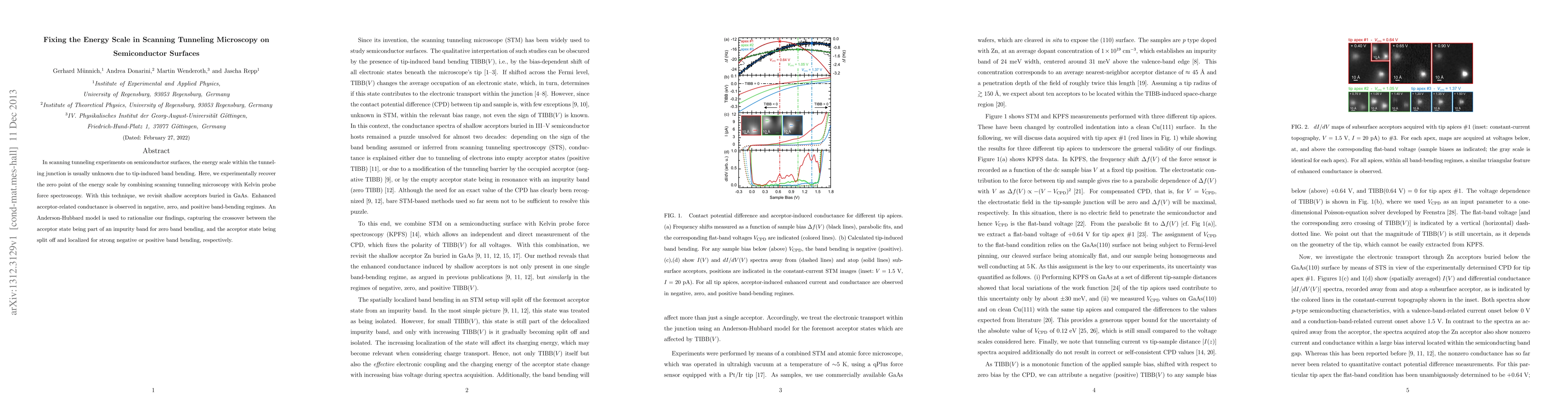
Fixing the Energy Scale in Scanning Tunneling Microscopy on Semiconductor Surfaces
Publication
Metrics
AI Quick Summary
This paper presents a method to determine the energy scale in scanning tunneling microscopy on semiconductor surfaces by integrating it with Kelvin probe force spectroscopy, allowing for the observation of enhanced acceptor-related conductance in GaAs across different band-bending regimes. The findings are explained using an Anderson-Hubbard model, which describes the transition of acceptor states under varying band bending conditions.
Paper Preview
Abstract
In scanning tunneling experiments on semiconductor surfaces, the energy scale within the tunneling junction is usually unknown due to tip-induced band bending. Here, we experimentally recover the zero point of the energy scale by combining scanning tunneling microscopy with Kelvin probe force spectroscopy. With this technique, we revisit shallow acceptors buried in GaAs. Enhanced acceptor-related conductance is observed in negative, zero, and positive band-bending regimes. An Anderson-Hubbard model is used to rationalize our findings, capturing the crossover between the acceptor state being part of an impurity band for zero band bending, and the acceptor state being split off and localized for strong negative or positive band bending, respectively.
AI Key Findings
Get AI-generated insights about this paper's methodology, results, significance, and more — seven facets brought into focus.
Impact
Paper Details
PDF Preview
Key Terms
Citation Network
Current paper (gray), citations (green), references (blue)
Display is limited for performance on very large graphs.
Discussion 0