This paper uses density functional theory to analyze how fluorination affects the structural stability and electronic properties of sp3 silicon nanotubes, finding that increased fluorine coverage enhances stability and lowers bandgaps, especially in low silicon molar fraction systems. Mixed fluorination and hydrogenation result in intermediate bandgaps.
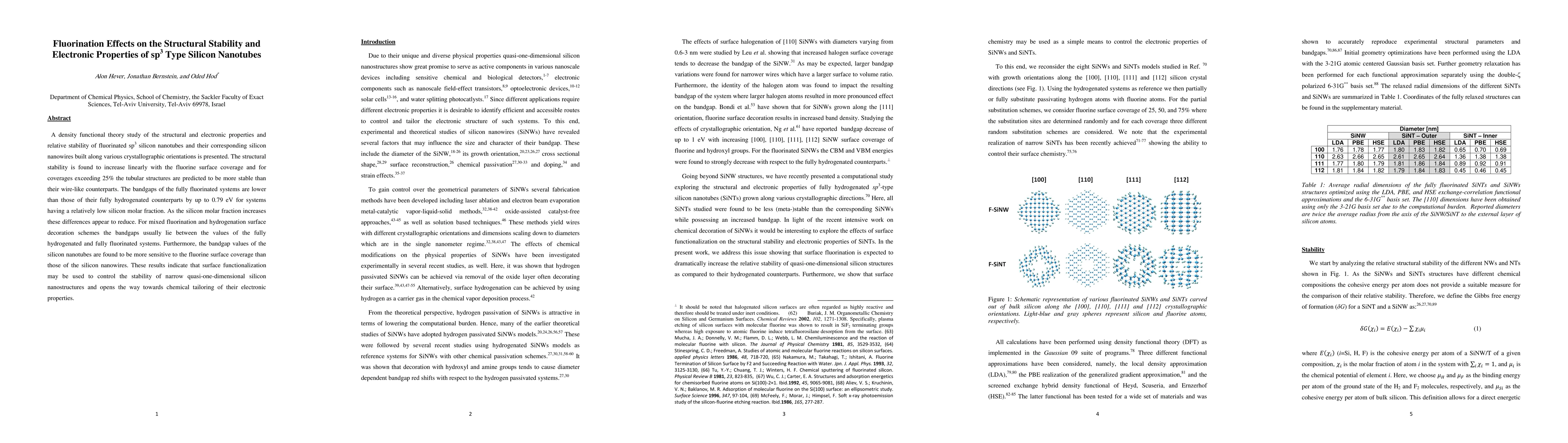
A density functional theory study of the structural and electronic properties and relative stability of fluorinated sp3 silicon nanotubes and their corresponding silicon nanowires built along various crystallographic orientations is presented. The structural stability is found to increase linearly with the fluorine surface coverage and for coverages exceeding 25% the tubular structures are predicted to be more stable than their wire-like counterparts. The bandgaps of the fully fluorinated systems are lower than those of their fully hydrogenated counterparts by up to 0.79 eV for systems having a relatively low silicon molar fraction. As the silicon molar fraction increases these differences appear to reduce. For mixed fluorination and hydrogenation surface decoration schemes the bandgaps usually lie between the values of the fully hydrogenated and fully fluorinated systems. Furthermore, the bandgap values of the silicon nanotubes are found to be more sensitive to the fluorine surface coverage than those of the silicon nanowires. These results indicate that surface functionalization may be used to control the stability of narrow quasi-one-dimensional silicon nanostructures and opens the way towards chemical tailoring of their electronic properties.
This graph shows how this paper is connected to other research. The current paper is shown in dark gray, papers that cite it are in green, and papers it references are in blue. You can:
• Hover over any node to see the paper title
• Click a node to view that paper's details
• Drag nodes to rearrange the graph
• Use the zoom controls (bottom right) to zoom in/out
No citations found for this paper.
Title | Authors | Year | Actions |
---|---|---|---|
Structural stability and electronic properties of sp3 type silicon nanotubes.
|
A. Hever, J. Bernstein, O. Hod
|
2012
|
View Paper |
Physics-Based Band Gap Model for Relaxed and Strained [100] Silicon Nanowires
|
R. Ghosh, S. Bhattacharya, S. Mahapatra
|
2012
|
View Paper |
Edge effect on band gap shift in Si nanowires with polygonal cross-sections
|
Ziming Zhu, Ai Zhang, G. Ouyang, Guowei Yang
|
2011
|
View Paper |
Surface and Electronic Properties of Hydrogen Terminated Si (001) Nanowires
|
Y. Matsuda, J. Tahir-Kheli, W. Goddard
|
2011
|
View Paper |
Electronic transport in natively oxidized silicon nanowires.
|
M. Koleini, L. Colombi Ciacchi, M. Fernandez-Serra
|
2011
|
View Paper |
Accurate prediction of the electronic properties of low-dimensional graphene derivatives using a screened hybrid density functional.
|
V. Barone, O. Hod, J. Peralta, G. Scuseria
|
2011
|
View Paper |
First-principles study of the structural, electronic, and optical properties of oxide-sheathed silicon nanowires.
|
R. Bondi, Sangheon Lee, G. Hwang
|
2011
|
View Paper |
Prediction of Silicon Nanowires as Photocatalysts for Water Splitting: Band Structures Calculated Using Density Functional Theory
|
Renqin Zhang, Xiaoming Liu, Z. Wen, Q. Jiang
|
2011
|
View Paper |
Wall-selective chemical alteration of silicon nanotube molecular carriers.
|
Moshit Ben-Ishai, F. Patolsky
|
2011
|
View Paper |
Supersensitive detection of explosives by silicon nanowire arrays.
|
Yoni Engel, R. Elnathan, A. Pevzner, Guy Davidi, E. Flaxer, F. Patolsky
|
2010
|
View Paper |
Enhanced absorption and carrier collection in Si wire arrays for photovoltaic applications.
|
M. Kelzenberg, S. Boettcher, J. Petykiewicz, D. Turner-Evans, M. C. Putnam, E. Warren, Joshua M. Spurgeon, R. Briggs, N. Lewis, H. Atwater
|
2010
|
View Paper |
Semiconductor nanowires for energy conversion
|
P. Yang
|
2010
|
View Paper |
Silicon nanowire band gap modification.
|
M. Nolan, S. O'Callaghan, G. Fagas, J. Greer, T. Frauenheim
|
2010
|
View Paper |
Surface passivation and transfer doping of silicon nanowires.
|
Chunsheng Guo, L. Luo, G. Yuan, Xiao-Bao Yang, Ruiqin Q. Zhang, Wen-Jun Zhang, Shui-Tong Lee
|
2009
|
View Paper |
Shape-tunable electronic properties of monohydride and trihydride [112]-oriented Si nanowires
|
A. Hmiel, Yongqiang Xue
|
2009
|
View Paper |
Control of growth mechanisms and orientation in epitaxial Si nanowires grown by electron beam evaporation
|
A. Irrera, E. Pecora, F. Priolo
|
2009
|
View Paper |
Single-crystal, Si nanotubes, and their mechanical resonant properties.
|
N. Quitoriano, M. Belov, S. Evoy, T. Kamins
|
2009
|
View Paper |
Shape- and dimension-controlled single-crystalline silicon and SiGe nanotubes: toward nanofluidic FET devices.
|
Moshit Ben Ishai, F. Patolsky
|
2009
|
View Paper |
Ab initio calculations of the mechanical and electronic properties of strained Si nanowires
|
Paul W. Leu, A. Svizhenko, Kyeongjae Cho
|
2008
|
View Paper |
Tunable electronic band structures of hydrogen-terminated ⟨112⟩ silicon nanowires
|
A. Lu, Ruiqin Q. Zhang, S. T. Lee
|
2008
|
View Paper |
Silicon nanowire array photoelectrochemical solar cells
|
Kui‐Qing Peng, Xin Wang, Shui-Tong Lee
|
2008
|
View Paper |
Strain-driven electronic band structure modulation of si nanowires.
|
K. Hong, Jongseob Kim, Sung-Hoon Lee, J. Shin
|
2008
|
View Paper |
Atomic and electronic structures of doped silicon nanowires : A first-principles study
|
E. Durgun, N. Akman, C. Ataca, S. Ciraci
|
2007
|
View Paper |
Unique electronic band structures of hydrogen-terminated silicon nanowires
|
A. Lu, R. Q. Zhang, S. T. Lee
|
2007
|
View Paper |
Theoretical investigation of silicon nanowires: Methodology, geometry, surface modification, and electrical conductivity using a multiscale approach
|
M. Ng, Liping Zhou, Shuo‐Wang Yang, Li Yun Sim, V. Tan, P. Wu
|
2007
|
View Paper |
Theoretical study of the chemical gap tuning in silicon nanowires
|
B. Aradi, L. Ramos, P. Deák, T. Köhler, F. Bechstedt, Ruiqin Q. Zhang, T. Frauenheim
|
2007
|
View Paper |
Enhanced half-metallicity in edge-oxidized zigzag graphene nanoribbons.
|
O. Hod, V. Barone, J. Peralta, G. Scuseria
|
2007
|
View Paper |
Silicon nanowire arrays for label-free detection of DNA.
|
Zhiqiang Gao, A. Agarwal, A. Trigg, Navab Singh, C. Fang, C. Tung, Yi Fan, K. Buddharaju, J. Kong
|
2007
|
View Paper |
Fabrication of silicon nanowire devices for ultrasensitive, label-free, real-time detection of biological and chemical species
|
F. Patolsky, Gengfeng Zheng, Charles M. Lieber
|
2006
|
View Paper |
Nanowire electronic and optoelectronic devices
|
Yat Li, Fang Qian, J. Xiang, Charles M. Lieber
|
2006
|
View Paper |
First principles simulations of the structural and electronic properties of silicon nanowires
|
T. Vo, A. Williamson, G. Galli
|
2006
|
View Paper |
Electrical characteristics and chemical stability of non-oxidized, methyl-terminated silicon nanowires.
|
H. Haick, P. Hurley, A. Hochbaum, P. Yang, N. Lewis
|
2006
|
View Paper |
Erratum: “Hybrid functionals based on a screened Coulomb potential” [J. Chem. Phys. 118, 8207 (2003)]
|
J. Heyd, G. Scuseria, M. Ernzerhof
|
2006
|
View Paper |
Surface chemical control of the electronic structure of silicon nanowires: Density functional calculations
|
Paul W. Leu, B. Shan, Kyeongjae Cho
|
2006
|
View Paper |
Effects of Morphology and Doping on the Electronic and Structural Properties of Hydrogenated Silicon Nanowires
|
A. Singh, Vijay Kumar, Y. Kawazoe
|
2006
|
View Paper |
Nanotechnologies for biomolecular detection and medical diagnostics.
|
M. Cheng, G. Cuda, Y. Bunimovich, M. Gaspari, J. Heath, H. Hill, C. Mirkin, A. J. Nijdam, R. Terracciano, T. Thundat, M. Ferrari
|
2006
|
View Paper |
Structure, stability, and quantum conductivity of small diameter silicon nanowires.
|
I. Ponomareva, M. Menon, D. Srivastava, A. Andriotis
|
2005
|
View Paper |
Energy band gaps and lattice parameters evaluated with the Heyd-Scuseria-Ernzerhof screened hybrid functional.
|
J. Heyd, J. Peralta, G. Scuseria, R. L. Martin
|
2005
|
View Paper |
Structures and energetics of hydrogen-terminated silicon nanowire surfaces.
|
Ruiqin Q. Zhang, Y. Lifshitz, D. D. D. Ma, Y. Zhao, T. Frauenheim, Shui-Tong Lee, S. Tong
|
2005
|
View Paper |
Sawtooth faceting in silicon nanowires.
|
F. Ross, J. Tersoff, M. Reuter
|
2005
|
View Paper |
Scanning photocurrent imaging and electronic band studies in silicon nanowire field effect transistors.
|
Y. Ahn, J. Dunning, Jiwoong Park
|
2005
|
View Paper |
Experimental imaging of silicon nanotubes
|
M. Crescenzi, P. Castrucci, M. Scarselli, M. Diociaiuti, P. Chaudhari, C. Balasubramanian, T. Bhave, S. Bhoraskar
|
2005
|
View Paper |
Self‐Assembled Silicon Nanotubes Grown from Silicon Monoxide
|
Y.-W. Chen, Y. Tang, L. Pei, C. Guo
|
2005
|
View Paper |
Efficient hybrid density functional calculations in solids: assessment of the Heyd-Scuseria-Ernzerhof screened Coulomb hybrid functional.
|
J. Heyd, G. Scuseria
|
2004
|
View Paper |
Quantum confinement and electronic properties of silicon nanowires.
|
Xinyuan Zhao, Ching-Ming Wei, Li Yang, M. Chou
|
2004
|
View Paper |
Assessment and validation of a screened Coulomb hybrid density functional.
|
J. Heyd, G. Scuseria
|
2004
|
View Paper |
Controlled Growth and Structures of Molecular-Scale Silicon Nanowires
|
Yue Wu, Yi Cui, L. Huynh, C. Barrelet, D. Bell, Charles M. Lieber
|
2004
|
View Paper |
Gold-catalyzed growth of silicon nanowires by plasma enhanced chemical vapor deposition
|
S. Hofmann, C. Ducati, R. Neill, S. Piscanec, A. Ferrari, J. Geng, R. Dunin‐Borkowski, J. Robertson
|
2003
|
View Paper |
Silicon-silica nanowires, nanotubes, and biaxial nanowires: inside, outside, and side-by-side growth of silicon versus silica on zeolite.
|
B. Teo, C. P. Li, X. Sun, N. Wong, S. Lee
|
2003
|
View Paper |
Synthesis of Silicon Nanotubes on Porous Alumina Using Molecular Beam Epitaxy
|
S. Jeong, Jae Yon Kim, Hyun Duk Yang, Bin Nal Yoon, S. Choi, H. Kang, Cheol‐Woong Yang, Young Hee Lee
|
2003
|
View Paper |
Structure and energetics of single-walled armchair and zigzag silicon nanotubes
|
A. S. Barnard, S. Russo
|
2003
|
View Paper |
Hybrid functionals based on a screened Coulomb potential
|
J. Heyd, G. Scuseria, M. Ernzerhof
|
2003
|
View Paper |
Small-Diameter Silicon Nanowire Surfaces
|
D. D. D. Ma, C. S. Lee, F. C. Au, S. Tong, S. Lee
|
2003
|
View Paper |
Organometallic chemistry on silicon and germanium surfaces.
|
J. Buriak
|
2002
|
View Paper |
Recent developments in silicon optoelectronic devices
|
H. Wong
|
2002
|
View Paper |
Logic Gates and Computation from Assembled Nanowire Building Blocks
|
Yu Huang, X. Duan, Yi Cui, L. Lauhon, Kyoung-Ha Kim, Charles M. Lieber
|
2001
|
View Paper |
Nanowire Nanosensors for Highly Sensitive and Selective Detection of Biological and Chemical Species
|
Yi Cui, Qingqiao Wei, Hongkun Park, Charles M. Lieber
|
2001
|
View Paper |
Proton/Protein Transport
|
G. Chin
|
2001
|
View Paper |
Diameter-controlled synthesis of single-crystal silicon nanowires
|
Yi Cui, L. Lauhon, M. Gudiksen, Jianfang Wang, Charles M. Lieber
|
2001
|
View Paper |
Nanotechnology: Thin solid films roll up into nanotubes
|
O. Schmidt, K. Eberl
|
2001
|
View Paper |
Direct synthesis of silicon nanowires, silica nanospheres, and wire-like nanosphere agglomerates
|
J. Gole, J. D. Stout, W. Rauch, Zhong Lin Wang
|
2000
|
View Paper |
Control of thickness and orientation of solution-grown silicon nanowires
|
J. Holmes, K. Johnston, R. C. Doty, B. Korgel
|
2000
|
View Paper |
One-dimensional growth mechanism of crystalline silicon nanowires
|
Yafei Zhang, Y. H. Tang, Ning Wang, Chun‐Sing Lee, I. Bello, Shui-Tong Lee
|
1999
|
View Paper |
Si nanowires grown from silicon oxide
|
Ning Wang, Y. H. Tang, Yafei Zhang, Chun‐Sing Lee, I. Bello, Shui-Tong Lee
|
1999
|
View Paper |
NUCLEATION AND GROWTH OF SI NANOWIRES FROM SILICON OXIDE
|
Ning Wang, Y. H. Tang, Yafei Zhang, Chun‐Sing Lee, Shui-Tong Lee
|
1998
|
View Paper |
Nanoscale silicon wires synthesized using simple physical evaporation
|
D. Yu, Z. Bai, Y. Ding, Q. Hang, Hongzhou Zhang, Jiajian Wang, Y. Zou, W. Qian, G. Xiong, Huanping Zhou, S. Feng
|
1998
|
View Paper |
Silicon nanowires prepared by laser ablation at high temperature
|
Yong Zhang, Y. H. Tang, Ning Wang, D. Yu, Chun‐Sing Lee, I. Bello, Shui-Tong Lee
|
1998
|
View Paper |
A laser ablation method for the synthesis of crystalline semiconductor nanowires
|
A. Morales, Charles M. Lieber
|
1998
|
View Paper |
Generalized Gradient Approximation Made Simple.
|
J. Perdew, K. Burke, M. Ernzerhof
|
1996
|
View Paper |
Validity of effective mass theory for energy levels in Si quantum wires
|
S. Horiguchi
|
1996
|
View Paper |
Adsorption of molecular fluorine on the Si(100) surface : an ellipsometric study
|
V. Aliev, V. Kruchinin, M. Baklanov
|
1996
|
View Paper |
Size dependence of band gaps in silicon nanostructures
|
B. Delley, E. F. Steigmeier
|
1995
|
View Paper |
Confinement, surface, and chemisorption effects on the optical properties of Si quantum wires.
|
Yeh, Zhang, Zunger
|
1994
|
View Paper |
Self‐limiting oxidation for fabricating sub‐5 nm silicon nanowires
|
H. I. Liu, D. Biegelsen, F. Ponce, N. Johnson, R. Pease
|
1994
|
View Paper |
Fluorine Termination of Silicon Surface by F2 and Succeeding Reaction with Water
|
M. Nakamura, Takayuki Takahagi Takayuki Takahagi, Akira Ishitani Akira Ishitani
|
1993
|
View Paper |
First-principles calculations of the electronic properties of silicon quantum wires.
|
Read, Needs, Nash, Canham, Calcott, Qteish
|
1992
|
View Paper |
Structures and adsorption energetics for chemisorbed fluorine atoms on Si(100)-2 x 1.
|
Wu, Carter
|
1992
|
View Paper |
Mechanism of HF etching of silicon surfaces: A theoretical understanding of hydrogen passivation.
|
G. Trucks, K. Raghavachari, G. Higashi, Y. Chabal
|
1990
|
View Paper |
Studies of atomic and molecular fluorine reactions on silicon surfaces
|
C. Stinespring, A. Freedman
|
1986
|
View Paper |
Chemiluminescence and the reaction of molecular fluorine with silicon
|
J. Mucha, V. M. Donnelly, D. Flamm, L. M. Webb
|
1981
|
View Paper |
Bond dissociation energy values in silicon-containing compounds and some of their implications
|
R. Walsh
|
1981
|
View Paper |
Chemical sputtering of fluorinated silicon
|
Y. Tu, T. Chuang, H. F. Winters
|
1981
|
View Paper |
Accurate spin-dependent electron liquid correlation energies for local spin density calculations: a critical analysis
|
S. H. Vosko, L. Wilk, M. Nusair
|
1980
|
View Paper |
The influence of polarization functions on molecular orbital hydrogenation energies
|
P. C. Hariharan, J. Pople
|
1973
|
View Paper |
2 Interfacing Biomolecules, Cells and Tissues with Nanowire-based Electrical Devices
|
Moria Kwiat, F. Patolsky
|
2012
|
View Paper |
Single nanowire photovoltaics.
|
B. Tian, T. Kempa, Charles M. Lieber
|
2009
|
View Paper |
Supercell Approach in Tight-Binding Calculation of Si and Ge Nanowire Bandstructures
|
管曦萌, 余志平
|
2005
|
View Paper |
Direct ultrasensitive electrical detection of DNA and DNA sequence variations using nanowire nanosensors
|
Jong-in Hahm and, Charles M. Lieber
|
2004
|
View Paper |
High Performance Silicon Nanowire Field Effect Transistors
|
Yi Cui, Z. Zhong, Deli Wang, Wayne U. Wang, Charles M. Lieber
|
2003
|
View Paper |
Soft X-ray photoemission study of the silicon-fluorine etching reaction
|
F. Mcfeely, J. Morar, F. Himpsel
|
1986
|
View Paper |
Showing first page preview. Click "Open Full PDF" to view the complete paper.
You need to log in to post a comment.
Your comment contains inappropriate language.
Are you sure you want to remove this tag?
Someone just favorited a paper!
Comments (0)