ArxivLens

Publication

Published: Jan 13, 2026
Categories: cond-mat.mtrl-sci

Metrics

Source: ArXiv

Quick Answers

What methodology did the authors use?

The research employs a combination of molecular beam epitaxy (MBE) and advanced characterization techniques such as X-ray diffraction (XRD), photoluminescence (PL), and transmission electron microscopy (TEM) to fabricate and analyze ultrathin GaN/AlN superlattices. More in Methodology →

What are the key results?

Achieved sub-240 nm emission wavelengths with high efficiency — Demonstrated self-limiting growth mechanisms for monolayer-scale structures More in Key Results →

Why is this work significant?

This work advances deep ultraviolet optoelectronics by enabling precise control over nanoscale semiconductor structures, which is critical for applications in UV communication, sensing, and sterilization. More in Significance →

What are the main limitations?

Scalability challenges in large-area fabrication — Limited understanding of long-term stability under operational conditions More in Limitations →

Paper Preview

Abstract

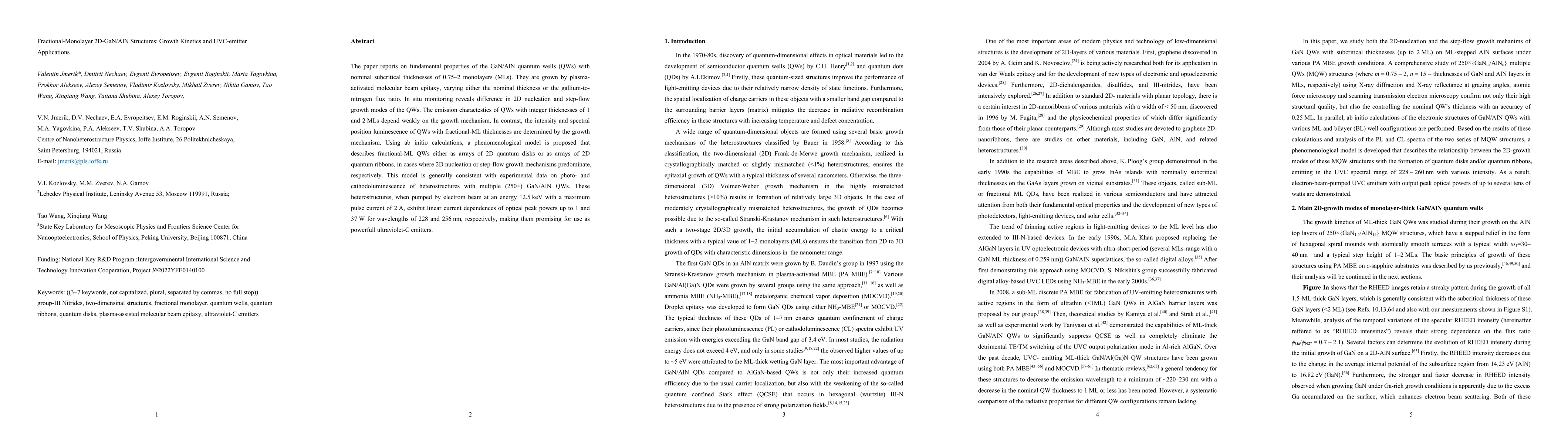
The paper reports on fundamental properties of the GaN/AlN quantum wells (QWs) with nominal subcritical thicknesses of 0.75-2 monolayers (MLs). They are grown by plasma-activated molecular beam epitaxy, varying either the nominal thickness or the gallium-to-nitrogen flux ratio. In situ monitoring reveals difference in 2D nucleation and step-flow growth modes of the QWs. The emission charactestics of QWs with integer thicknesses of 1 and 2 MLs depend weakly on the growth mechanism. In contrast, the intensity and spectral position luminescence of QWs with fractional-ML thicknesses are determined by the growth mechanism. Using ab initio calculations, a phenomenological model is proposed that describes fractional-ML QWs either as arrays of 2D quantum disks or as arrays of 2D quantum ribbons, in cases where 2D nucleation or step-flow growth mechanisms predominate, respectively. This model is generally consistent with experimental data on photo- and cathodoluminescence of heterostructures with multiple (250) GaN/AlN QWs. These heterostructures, when pumped by electrom beam at an energy 12.5 keV with a maximum pulse current of 2 A, exhibit linear current dependences of optical peak powers up to 1 and 37 W for wavelengths of 228 and 256 nm, respectively, making them promising for use as powerfull ultraviolet-C emitters.

Key Findings, in focus

Seven facets of this paper, analysed and brought into focus by AI.

AI-generated · verify against source Generated Jan 14, 2026
In focus · one-line synthesis

This work advances deep ultraviolet optoelectronics by enabling precise control over nanoscale semiconductor structures, which is critical for applications in UV communication, sensing, and sterilization.

01
MethodologyHow they did it

The research employs a combination of molecular beam epitaxy (MBE) and advanced characterization techniques such as X-ray diffraction (XRD), photoluminescence (PL), and transmission electron microscopy (TEM) to fabricate and analyze ultrathin GaN/AlN superlattices.

02
ResultsWhat they found
  • Achieved sub-240 nm emission wavelengths with high efficiency
  • Demonstrated self-limiting growth mechanisms for monolayer-scale structures
  • Observed enhanced optical properties due to quantum confinement effects
03
SignificanceWhy it matters

This work advances deep ultraviolet optoelectronics by enabling precise control over nanoscale semiconductor structures, which is critical for applications in UV communication, sensing, and sterilization.

04
Technical ContributionsWhat's new technically

Development of hierarchical growth units for integral monolayer-scale digital-alloyed AlN/GaN superlattices

05
NoveltyWhat sets it apart

Integration of self-limiting growth with digital alloying to achieve atomic-scale precision in semiconductor heterostructures

06
LimitationsWhat to be cautious about
  • Scalability challenges in large-area fabrication
  • Limited understanding of long-term stability under operational conditions
07
Future WorkWhere it goes next
  • Exploring alternative growth techniques for scalable production
  • Investigating defect engineering to improve device reliability

Paper Details

Paper ID: 2601.08410
Comments: 32 pages, 5 fugures, regular article
Categories:
cond-mat.mtrl-sci

How to Cite This Paper

Reference manager: RIS EndNote


Discussion 0

This website uses cookies to ensure you get the best experience. Learn more