Authors
Summary
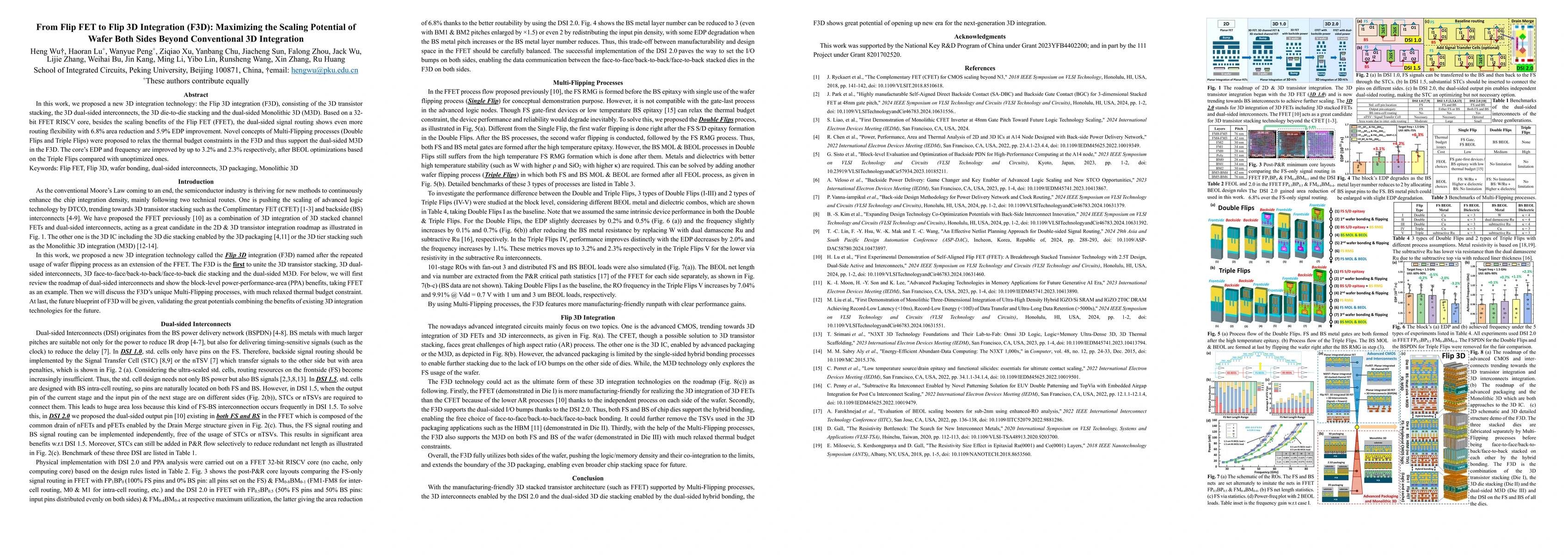
In this work, we proposed a new 3D integration technology: the Flip 3D integration (F3D), consisting of the 3D transistor stacking, the 3D dual-sided interconnects, the 3D die-to-die stacking and the dual-sided Monolithic 3D (M3D). Based on a 32-bit FFET RISCV core, besides the scaling benefits of the Flip FET (FFET), the dual-sided signal routing shows even more routing flexibility with 6.8% area reduction and 5.9% EDP improvement. Novel concepts of Multi-Flipping processes (Double Flips and Triple Flips) were proposed to relax the thermal budget constraints in the F3D and thus support the dual-sided M3D in the F3D. The core's EDP and frequency are improved by up to 3.2% and 2.3% respectively, after BEOL optimizations based on the Triple Flips compared with unoptimized ones.
AI Key Findings
Get AI-generated insights about this paper's methodology, results, and significance.
Paper Details
PDF Preview
Citation Network
Current paper (gray), citations (green), references (blue)
Display is limited for performance on very large graphs.
Similar Papers
Found 4 papersA Tale of Two Sides of Wafer: Physical Implementation and Block-Level PPA on Flip FET with Dual-sided Signals
Yibo Lin, Runsheng Wang, Ru Huang et al.
Design Optimization of Flip FET Standard Cells with Dual-sided Pins for Ultimate Scaling
Ming Li, Yibo Lin, Runsheng Wang et al.
| Title | Authors | Year | Actions |
|---|
Comments (0)