01
MethodologyHow they did it
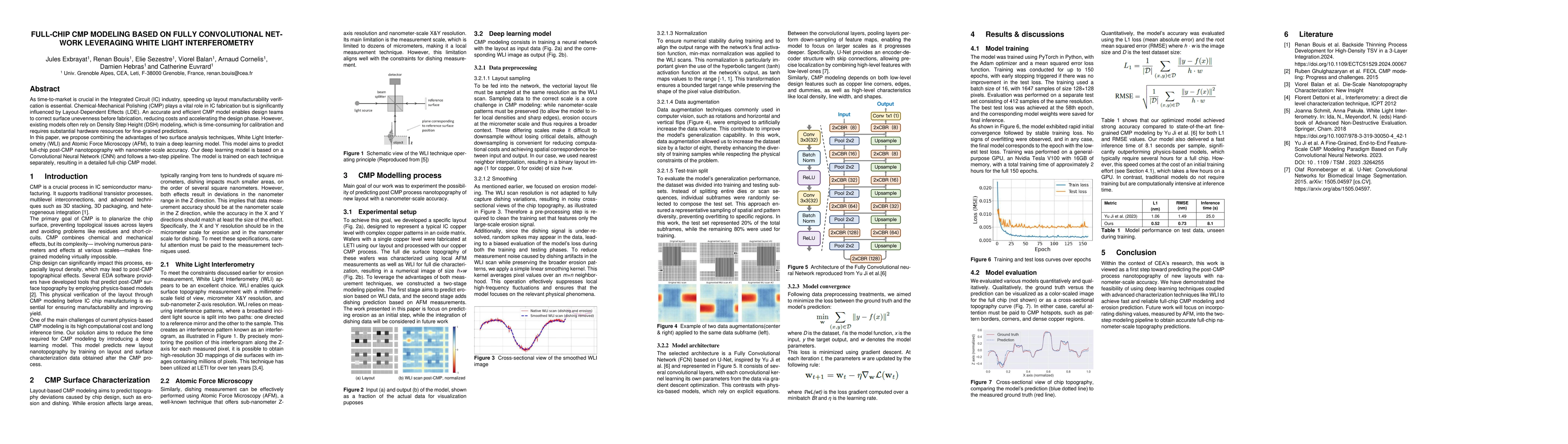
A two-stage deep learning pipeline is employed: first predicting erosion from White Light Interferometry (WLI) data, followed by incorporating dishing predictions from Atomic Force Microscopy (AFM) measurements; data preprocessing includes layout sampling to match WLI resolution and smoothing to reduce noise, training a CNN with layout as input and WLI image as output using PyTorch, Adam optimizer, MSE loss, and early stopping.
Discussion 0