Full loss compensation in hybrid plasmonic waveguides under electrical pumping
Publication
Metrics
Paper Preview
Abstract
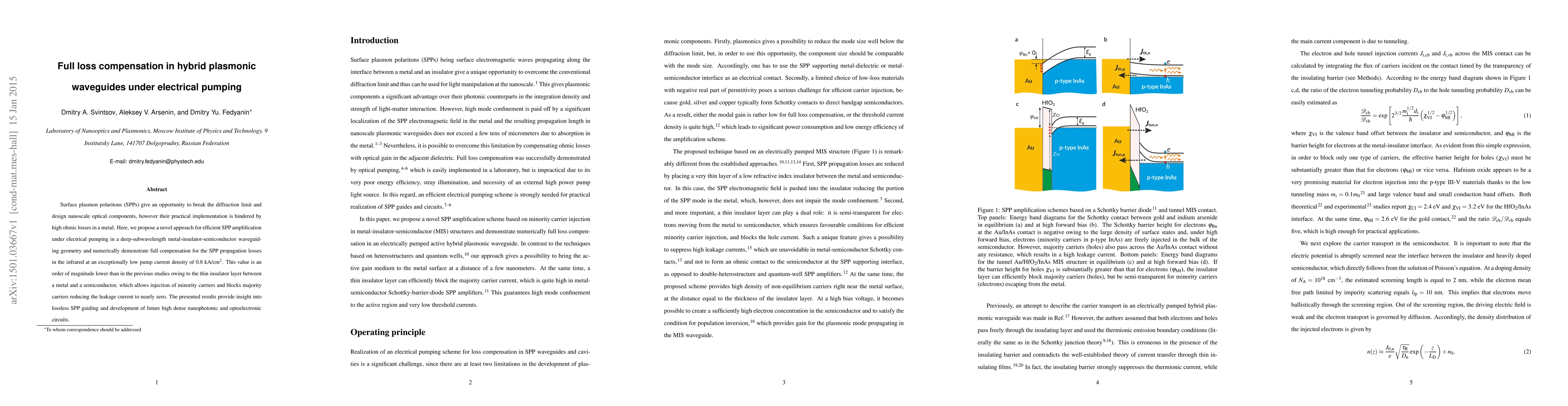
Surface plasmon polaritons (SPPs) give an opportunity to break the diffraction limit and design nanoscale optical components, however their practical implementation is hindered by high ohmic losses in a metal. Here, we propose a novel approach for efficient SPP amplification under electrical pumping in a deep-subwavelength metal-insulator-semiconductor waveguiding geometry and numerically demonstrate full compensation for the SPP propagation losses in the infrared at an exceptionally low pump current density of 0.8 kA/cm$^2$. This value is an order of magnitude lower than in the previous studies owing to the thin insulator layer between a metal and a semiconductor, which allows injection of minority carriers and blocks majority carriers reducing the leakage current to nearly zero. The presented results provide insight into lossless SPP guiding and development of future high dense nanophotonic and optoelectronic circuits.
AI Key Findings
Get AI-generated insights about this paper's methodology, results, significance, and more — seven facets brought into focus.
Impact
Paper Details
PDF Preview
Key Terms
Citation Network
Current paper (gray), citations (green), references (blue)
Display is limited for performance on very large graphs.
Discussion 0