Full orientation control of epitaxial MoS2 on hBN assisted by substrate defects
Publication
Metrics
Paper Preview
Abstract
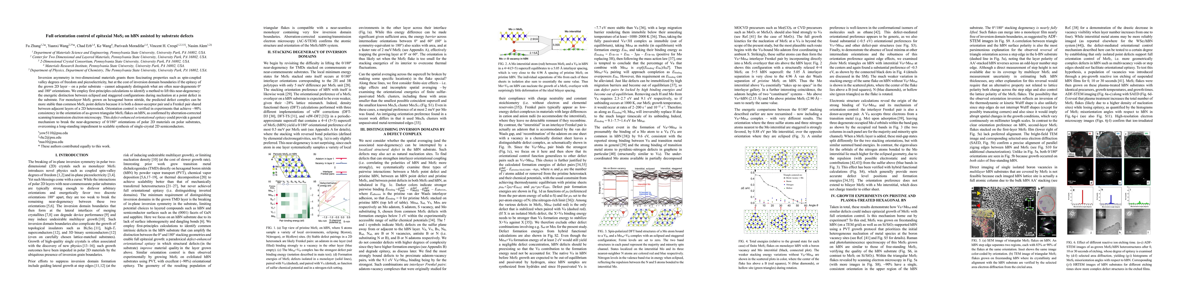
Inversion asymmetry in two-dimensional materials grants them fascinating properties such as spin-coupled valley degrees of freedom and piezoelectricity, but at the cost of inversion domain boundaries if the epitaxy of the grown 2D layer -- on a polar substrate -- cannot adequately distinguish what are often near-degenerate 0{\deg} and 180{\deg} orientations. We employ first-principles calculations to identify a method to lift this near-degeneracy: the energetic distinction between eclipsed and staggered configurations during nucleation at a point defect in the substrate. For monolayer MoS2 grown on hexagonal boron nitride, the predicted defect complex can be more stable than common MoS2 point defects because it is both a donor-acceptor pair and a Frenkel pair shared between adjacent layers of a 2D heterostack. Orientation control is verified in experiments that achieve ~90% consistency in the orientation of as-grown triangular MoS2 flakes on hBN, as confirmed by aberration-corrected scanning/transmission electron microscopy. This defect-enhanced orientational epitaxy could provide a general mechanism to break the near-degeneracy of 0/180{\deg} orientations of polar 2D materials on polar substrates, overcoming a long-standing impediment to scalable synthesis of single-crystal 2D semiconductors.
AI Key Findings
Get AI-generated insights about this paper's methodology, results, significance, and more — seven facets brought into focus.
Impact
Paper Details
PDF Preview
Key Terms
Citation Network
Current paper (gray), citations (green), references (blue)
Display is limited for performance on very large graphs.
Discussion 0