Fully automated spectroscopic ellipsometry analyses of crystalline-phase semiconductors based on a new algorithm
Publication
Metrics
AI Quick Summary
This paper introduces a fully automated spectroscopic ellipsometry (SE) analysis method for crystalline-phase semiconductors, significantly reducing analysis time by incorporating a new algorithm that automates the identification and fitting of multiple optical transition peaks. The proposed Delta M method has been successfully applied to perovskite-based samples, demonstrating its effectiveness in determining complex dielectric functions and structural parameters.
Paper Preview
Abstract
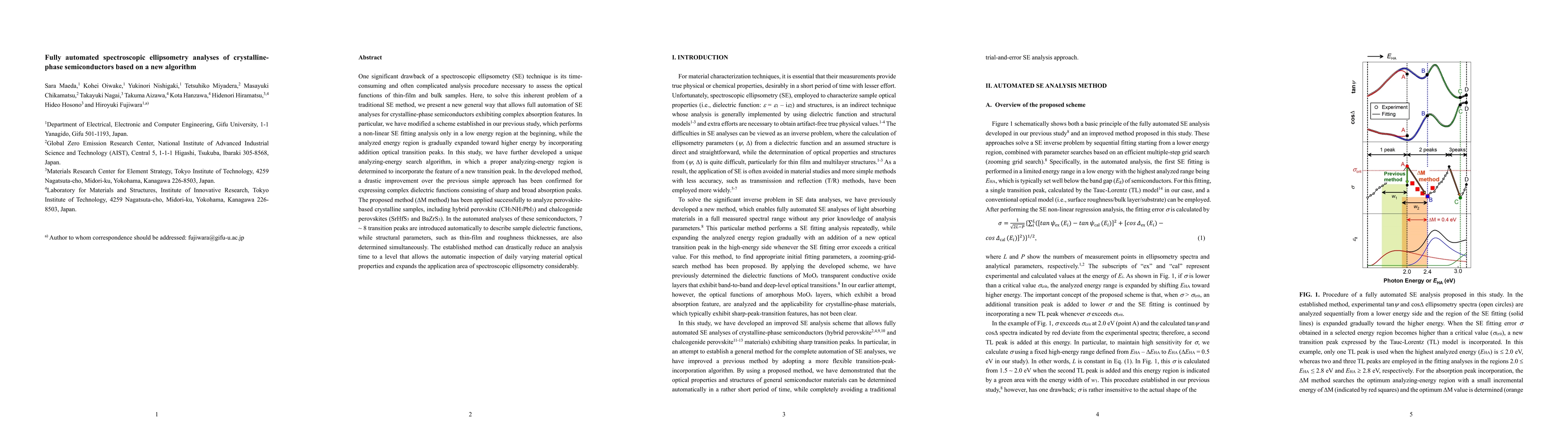
One significant drawback of a spectroscopic ellipsometry (SE) technique is its time-consuming and often complicated analysis procedure necessary to assess the optical functions of thin-film and bulk samples. Here, to solve this inherent problem of a traditional SE method, we present a new general way that allows full automation of SE analyses for crystalline-phase semiconductors exhibiting complex absorption features. In particular, we have modified a scheme established in our previous study, which performs a non-linear SE fitting analysis only in a low energy region at the beginning, while the analyzed energy region is gradually expanded toward higher energy by incorporating addition optical transition peaks. In this study, we have further developed a unique analyzing-energy search algorithm, in which a proper analyzing-energy region is determined to incorporate the feature of a new transition peak. In the developed method, a drastic improvement over the previous simple approach has been confirmed for expressing complex dielectric functions consisting of sharp and broad absorption peaks. The proposed method (Delta M method) has been applied successfully to analyze perovskite-based crystalline samples, including hybrid perovskite (CH3NH3PbI3) and chalcogenide perovskites (SrHfS3 and BaZrS3). In the automated analyses of these semiconductors, 7-8 transition peaks are introduced automatically to describe sample dielectric functions, while structural parameters, such as thin-film and roughness thicknesses, are also determined simultaneously. The established method can drastically reduce an analysis time to a level that allows the automatic inspection of daily varying material optical properties and expands the application area of spectroscopic ellipsometry considerably.
AI Key Findings
Get AI-generated insights about this paper's methodology, results, significance, and more — seven facets brought into focus.
Paper Details
Authors
PDF Preview
Key Terms
Related Papers
No references found for this paper.
Discussion 0