Functionalization of Single Layer MoS$_2$ Honeycomb Structures
Publication
Metrics
AI Quick Summary
This study utilizes first-principles calculations to investigate how the properties of single layer MoS$_2$ are altered via adatom adsorption and vacancy defects. Specific adatoms and triple vacancies induce magnetism and new charge states, expanding MoS$_2$'s applications in nanoelectronics, spintronics, and tribology.
Paper Preview
Abstract
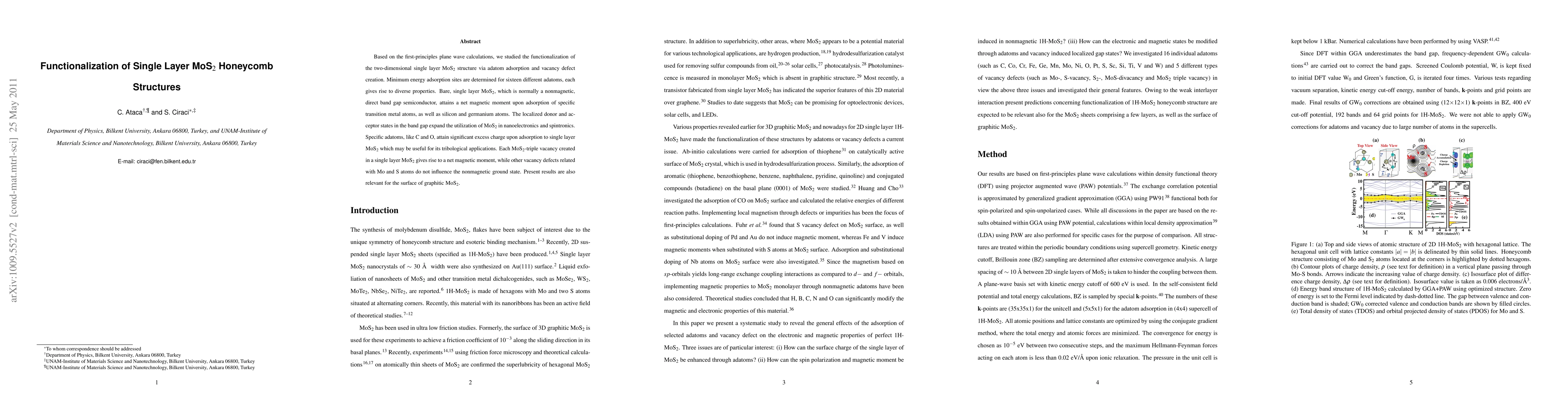
Based on the first-principles plane wave calculations, we studied the functionalization of the two-dimensional single layer MoS$_2$ structure via adatom adsorption and vacancy defect creation. Minimum energy adsorption sites are determined for sixteen different adatoms, each gives rise to diverse properties. Bare, single layer MoS$_2$, which is normally a nonmagnetic, direct band gap semiconductor, attains a net magnetic moment upon adsorption of specific transition metal atoms, as well as silicon and germanium atoms. The localized donor and acceptor states in the band gap expand the utilization of MoS$_2$ in nanoelectronics and spintronics. Specific adatoms, like C and O, attain significant excess charge upon adsorption to single layer MoS$_{2}$ which may be useful for its tribological applications. Each MoS$_{2}$-triple vacancy created in a single layer MoS$_{2}$ gives rise to a net magnetic moment, while other vacancy defects related with Mo and S atoms do not influence the nonmagnetic ground state. Present results are also relevant for the surface of graphitic MoS$_2$.
AI Key Findings
Get AI-generated insights about this paper's methodology, results, significance, and more — seven facets brought into focus.
Impact
Paper Details
PDF Preview
Key Terms
Citation Network
Current paper (gray), citations (green), references (blue)
Display is limited for performance on very large graphs.
Discussion 0