01
MethodologyHow they did it
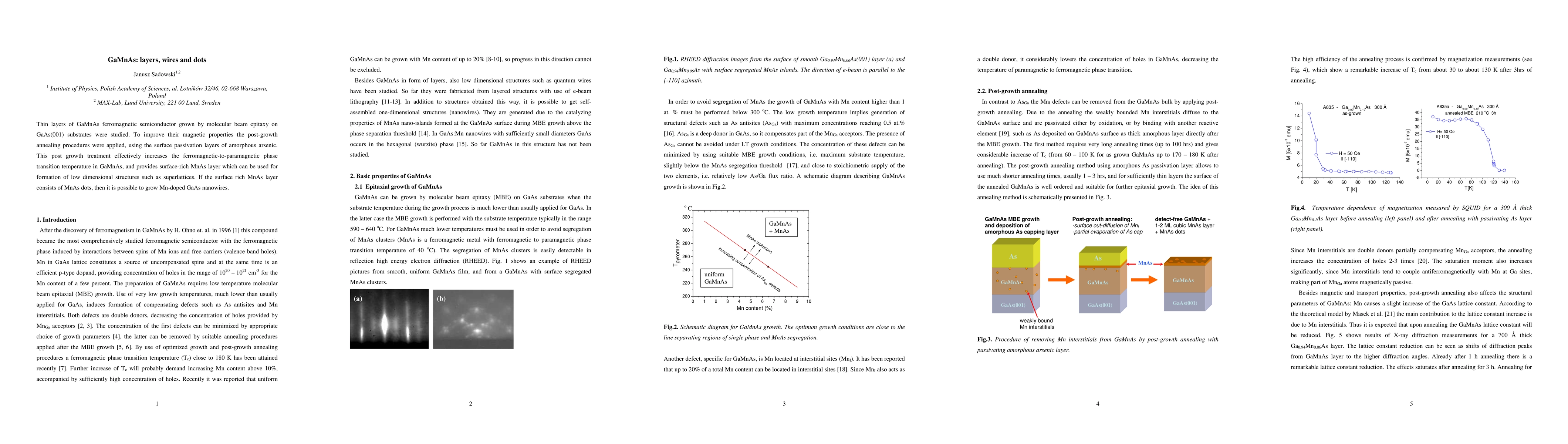
The research methodology involved growing thin layers of GaMnAs ferromagnetic semiconductor on GaAs(001) substrates using molecular beam epitaxy (MBE), followed by post-growth annealing with amorphous arsenic to enhance magnetic properties.
Discussion 0