Summary
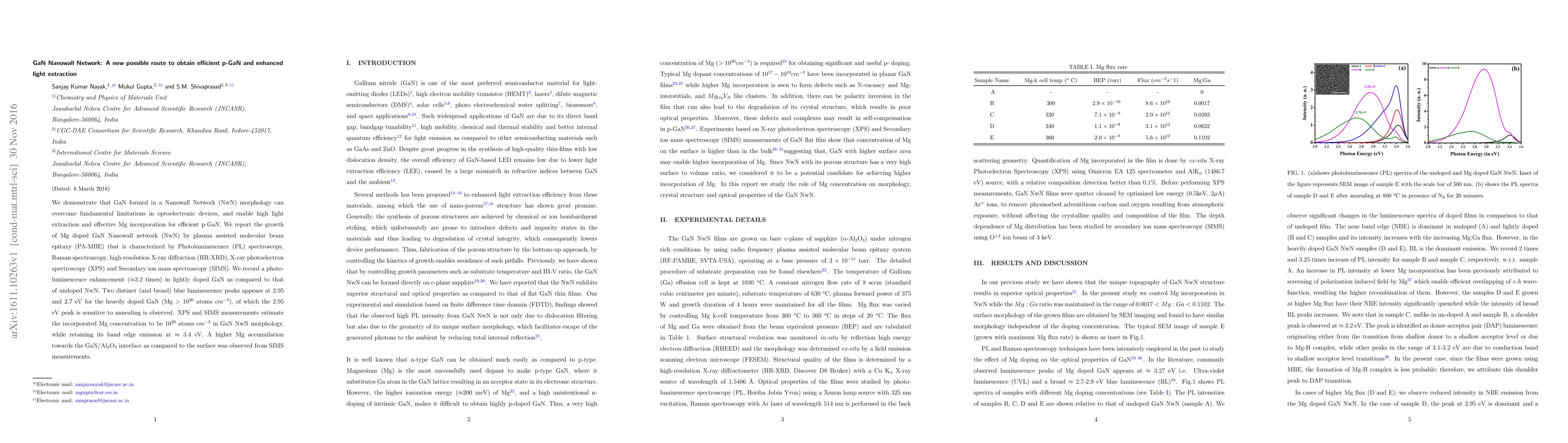
We demonstrate that GaN formed in a Nanowall Network (NwN) morphology can overcome fundamental limitations in optoelectronic devices, and enable high light extraction and effective Mg incorporation for efficient p-GaN. We report the growth of Mg doped GaN Nanowall network (NwN) by plasma assisted molecular beam epitaxy (PA-MBE) that is characterized by Photoluminescence (PL) spectroscopy, Raman spectroscopy, high-resolution X-ray diffraction (HR-XRD), X-ray photoelectron spectroscopy (XPS) and Secondary ion mass spectroscopy (SIMS). We record a photo-luminescence enhancement ($ \approx $3.2 times) in lightly doped GaN as compared to that of undoped NwN. Two distinct (and broad) blue luminescence peaks appears at 2.95 and 2.7 eV for the heavily doped GaN (Mg $>10^{20}$ atoms $cm^{-3}$), of which the 2.95 eV peak is sensitive to annealing is observed. XPS and SIMS measurements estimate the incorporated Mg concentration to be $10^{20}$ atoms $cm^{-3}$ in GaN NwN morphology, while retaining its band edge emission at $\approx$ 3.4 eV. A higher Mg accumulation towards the GaN/Al$_2$O$_3$ interface as compared to the surface was observed from SIMS measurements.
AI Key Findings
Get AI-generated insights about this paper's methodology, results, and significance.
Paper Details
PDF Preview
Key Terms
Citation Network
Current paper (gray), citations (green), references (blue)
Display is limited for performance on very large graphs.
Similar Papers
Found 4 papersNo citations found for this paper.
Comments (0)