Gap Engineered Superconducting Multilayer Nanobridge Josephson Junctions
Publication
Metrics
Paper Preview
Abstract
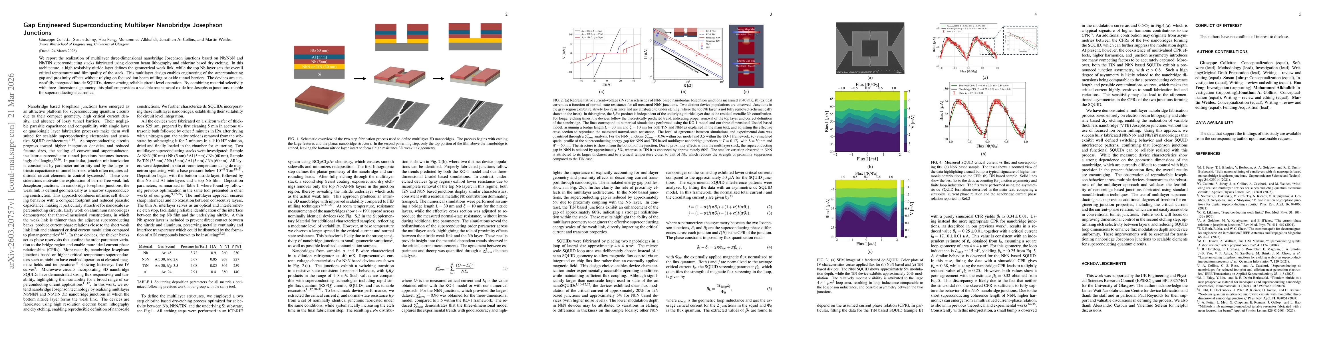
We report the realization of multilayer three-dimensional nanobridge Josephson junctions based on Nb/NbN and Nb/TiN superconducting stacks fabricated using electron-beam lithography and chlorine-based dry etching. In this architecture, a high-resistivity nitride layer defines the geometrical weak link, while the top Nb layer sets the overall critical temperature and film quality of the stack. This multilayer design enables engineering of the superconducting gap and proximity effects without relying on focused ion beam milling or oxide tunnel barriers. The devices are successfully integrated into dc SQUIDs, demonstrating reliable circuit-level operation. By combining material selectivity with three-dimensional geometry, this platform provides a scalable route toward oxide-free Josephson junctions suitable for superconducting electronics.
AI Key Findings
Get AI-generated insights about this paper's methodology, results, significance, and more — seven facets brought into focus.
Discussion 0