Summary
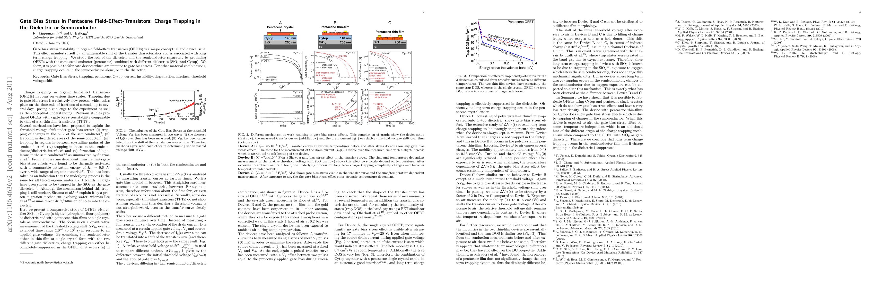
Gate bias stress instability in organic field-effect transistors (OFETs) is a major conceptual and device issue. This effect manifests itself by an undesirable shift of the transfer characteristics and is associated with long term charge trapping. We study the role of the dielectric and the semiconductor separately by producing OFETs with the same semiconductor (pentacene) combined with different dielectrics (SiO$_2$ and Cytop). We show, it is possible to fabricate devices which are immune to gate bias stress. For other material combinations, charge trapping occurs in the semiconductor alone, or in the dielectric.
AI Key Findings
Get AI-generated insights about this paper's methodology, results, and significance.
Paper Details
PDF Preview
Key Terms
Citation Network
Current paper (gray), citations (green), references (blue)
Display is limited for performance on very large graphs.
Similar Papers
Found 4 papers| Title | Authors | Year | Actions |
|---|

Comments (0)