Publication
Metrics
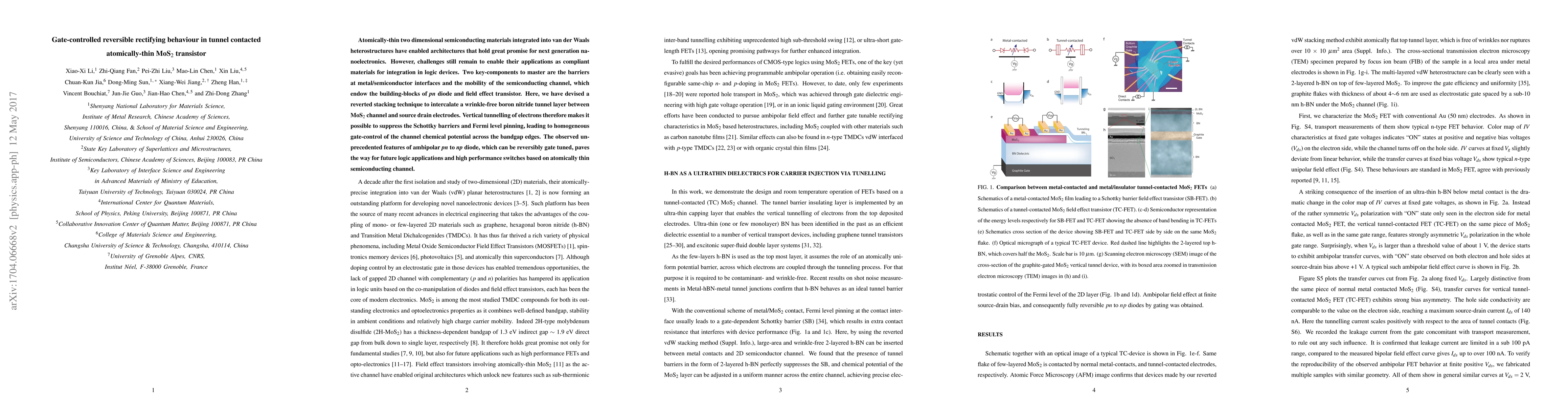
Paper Preview
Abstract
Atomically-thin 2D semiconducting materials integrated into van der Waals heterostructures have enabled architectures that hold great promise for next generation nanoelectronics. However, challenges still remain to enable their full acceptance as compliant materials for integration in logic devices. Two key-components to master are the barriers at metal/semiconductor interfaces and the mobility of the semiconducting channel, which endow the building-blocks of ${pn}$ diode and field effect transistor. Here, we have devised a reverted stacking technique to intercalate a wrinkle-free h-BN tunnel layer between MoS$_{2}$ channel and contacting electrodes. Vertical tunnelling of electrons therefore makes it possible to suppress the Schottky barriers and Fermi level pinning, leading to homogeneous gate-control of the channel chemical potential across the bandgap edges. The observed unprecedented features of ambipolar ${pn}$ to ${np}$ diode, which can be reversibly gate tuned, paves the way for future logic applications and high performance switches based on atomically thin semiconducting channel.
AI Key Findings
Get AI-generated insights about this paper's methodology, results, significance, and more — seven facets brought into focus.
Impact
Paper Details
PDF Preview
Key Terms
Citation Network
Current paper (gray), citations (green), references (blue)
Display is limited for performance on very large graphs.
Discussion 0