Publication
Metrics
AI Quick Summary
This paper reports on gate-tunable, high-mobility InSb/In_{1-x}Al_{x}Sb quantum wells with 2DEG channel mobility exceeding 200,000 cm^{2}/Vs at 1.8K, achieved using HfO_{2} gate dielectrics and demonstrating the integer quantum Hall effect.
Paper Preview
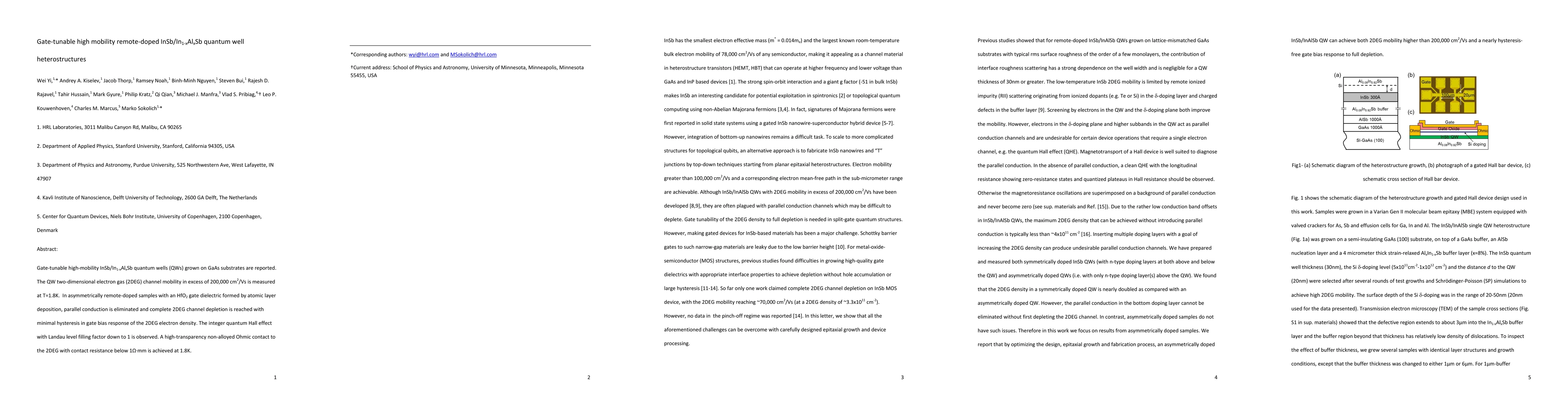
Abstract
Gate-tunable high-mobility InSb/In_{1-x}Al_{x}Sb quantum wells (QWs) grown on GaAs substrates are reported. The QW two-dimensional electron gas (2DEG) channel mobility in excess of 200,000 cm^{2}/Vs is measured at T=1.8K. In asymmetrically remote-doped samples with an HfO_{2} gate dielectric formed by atomic layer deposition, parallel conduction is eliminated and complete 2DEG channel depletion is reached with minimal hysteresis in gate bias response of the 2DEG electron density. The integer quantum Hall effect with Landau level filling factor down to 1 is observed. A high-transparency non-alloyed Ohmic contact to the 2DEG with contact resistance below 1{\Omega} \cdot mm is achieved at 1.8K.
AI Key Findings
Get AI-generated insights about this paper's methodology, results, significance, and more — seven facets brought into focus.
Impact
Paper Details
PDF Preview
Key Terms
Citation Network
Current paper (gray), citations (green), references (blue)
Display is limited for performance on very large graphs.
Discussion 0