ArxivLens

Quick Summary:

This study investigates the electric transport in bilayer graphene diodes with dual gate control, revealing non-linear currents and current rectification that can be tuned via gate voltages. The research identifies a gate-dependent bandgap ranging from 0 meV to 130 meV, showcasing the potential for gate-tunable pn junction characteristics.

DOI: 10.1063/1.3676441
arXiv Id: 1201.1105
Comments: 4 pages
Date Published: 2012-01-06
Date Updated: 2012-01-06

Categories:

Key Terms (TF-IDF):

gate (0.327)
bilayer (0.309)
junction (0.287)
graphene (0.260)
mev (0.236)
double (0.212)
fermi level (0.182)
charge density (0.173)
directional (0.173)
ranges (0.156)
voltage (0.150)
currents (0.148)
non linear (0.147)
create (0.144)
controlled (0.138)
extract (0.138)
locally (0.136)
fermi (0.133)
characterized (0.132)
electric (0.129)
License: http://arxiv.org/licenses/nonexclusive-distrib/1.0/

Summary:

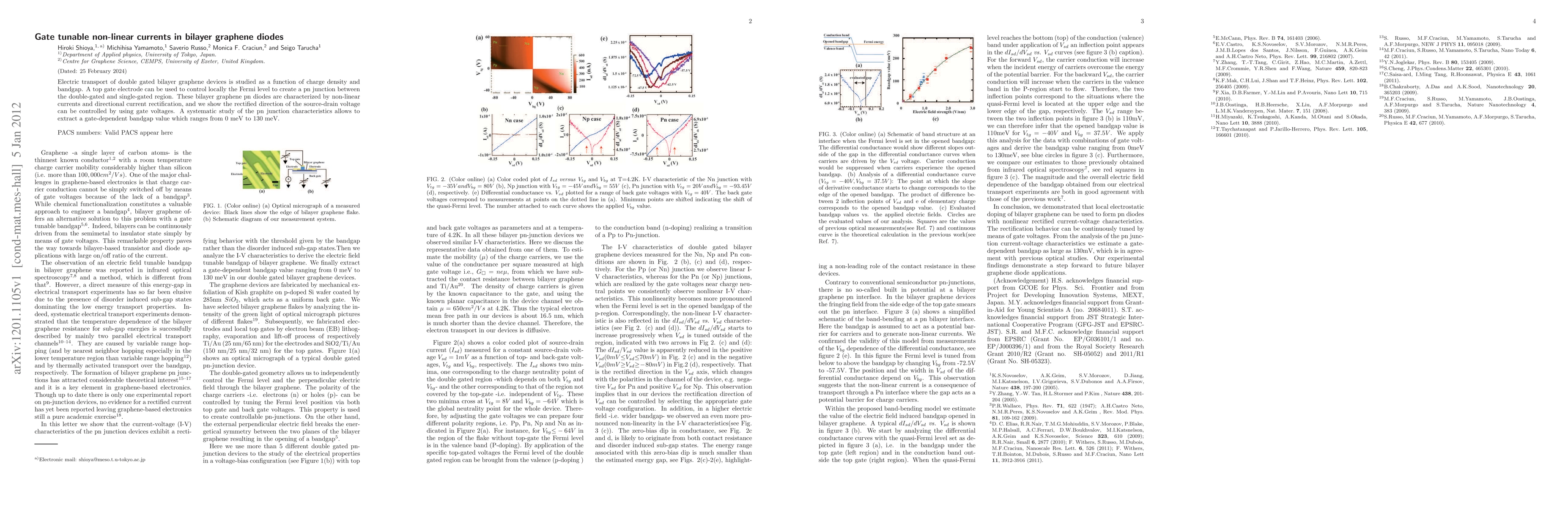
Electric transport of double gated bilayer graphene devices is studied as a function of charge density and bandgap. A top gate electrode can be used to control locally the Fermi level to create a pn junction between the double-gated and single-gated region. These bilayer graphene pn diodes are characterized by non-linear currents and directional current rectification, and we show the rectified direction of the source-drain voltage can be controlled by using gate voltages. A systematic study of the pn junction characteristics allows to extract a gate-dependent bandgap value which ranges from 0 meV to 130 meV.

Citation & Reference Network Visualization

This graph shows how this paper is connected to other research. The current paper is shown in dark gray, papers that cite it are in green, and papers it references are in blue. You can:

Current Paper
Papers citing this work (Citations)
Papers cited by this work (References)

• Hover over any node to see the paper title

• Click a node to view that paper's details

• Drag nodes to rearrange the graph

• Use the zoom controls (bottom right) to zoom in/out

Citations and References

Title Authors Year Actions
Transport Spectroscopy of Ultraclean Tunable Band Gaps in Bilayer Graphene
E. Icking, L. Banszerus, F. Wörtche, F. Volmer, Philipp Schmidt, Corinne Steiner, S. Engels, Jonas Hesselmann, M. Goldsche, Kenji Watanabe, T. Taniguchi, C. Volk, B. Beschoten, C. Stampfer
2022
View Paper
Effects of strain and electric fields on the electronic transport properties of single-layer β12-borophene nanoribbons.
M. Davoudiniya, K. Mirabbaszadeh
2021
View Paper
Spin transport properties in TM-doped B38 fullerene/borophene junctions
H. Khalatbari, S. Vishkayi, H. Soleimani
2021
View Paper
Charge transport in a molecule-borophene junction: The effect of junction configurations
H. Khalatbari, S. Vishkayi, H. Soleimani
2020
View Paper
Ion-Locking in Solid Polymer Electrolytes for Reconfigurable Gateless Lateral Graphene p-n Junctions
Jierui Liang, Ke Xu, S. Arora, Jennifer E. Laaser, Susan K. Fullerton‐Shirey
2020
View Paper
Bilayer Graphene Conductance Analysis based on FET Channel
V. Nazerian, M. J. Kiani
2018
View Paper
Is graphene a good transparent electrode for photovoltaics and display applications?
Thomas H. Bointon, S. Russo, M. Craciun
2015
View Paper
Valley Hall Effect in Two-Dimensional Hexagonal Lattices
M. Yamamoto, Y. Shimazaki, I. Borzenets, S. Tarucha
2015
View Paper
Achieving large transport bandgaps in bilayer graphene
T. Chu, Zhihong Chen
2015
View Paper
Reconfigurable p-n junction formation and bandgap opening in bilayer graphene using polyethylene oxide and CsClO4 solid polymer electrolyte
Ke Xu, T. Chu, B. Bourdon, A. Seabaugh, Zhihong Chen, Susan K. Fullerton‐Shirey
2015
View Paper
Direct Observation of a Gate Tunable Band Gap in Electrical Transport in ABC-Trilayer Graphene.
T. Khodkov, I. Khrapach, M. Craciun, S. Russo
2015
View Paper
Experimental study on SET/RESET conditions for graphene resistive random access memory
A. Shindome, Tsunaki Takahashi, S. Oda, K. Uchida
2014
View Paper
Semiconducting properties of bilayer graphene modulated by an electric field for next-generation atomic-film electronics
K. Tsukagoshi, S-L Li, Hidetoshi Miyazaki, A. Aparecido-Ferreira, S. Nakaharai
2014
View Paper
Straining Graphene Using Thin Film Shrinkage Methods
H. Shioya, M. Craciun, S. Russo, M. Yamamoto, S. Tarucha
2014
View Paper
Experimental Study of Two-Terminal Resistive Random Access Memory Realized in Mono- and Multilayer Exfoliated Graphene Nanoribbons
A. Shindome, Y. Doioka, N. Beppu, S. Oda, K. Uchida
2013
View Paper
Enhanced current-rectification in bilayer graphene with an electrically tuned sloped bandgap.
A. Aparecido-Ferreira, H. Miyazaki, Song-Lin Li, K. Komatsu, S. Nakaharai, K. Tsukagoshi
2012
View Paper
A disorder induced field effect transistor in bilayer and trilayer graphene
Dongwei Xu, Haiwen Liu, V. Sacksteder, Juntao Song, Hua Jiang, Qing-feng Sun, X. Xie
2012
View Paper
Electronic structure and trajectory control of Dirac fermions in graphene ribbons under the competition between electric and magnetic fields
Mou Yang, Yan Cui, Rui-Qiang Wang, Hongbo Zhao
2012
View Paper
Graphene and ZnO Nanostructures for Nano- Optoelectronic a Biosensing Applications
K. Hasan
2012
View Paper

Comments (0)

This website uses cookies to ensure you get the best experience. Learn more