Publication
Metrics
AI Quick Summary
This paper demonstrates gate-tunable 2D/3D van der Waals semiconductor heterojunctions using MoS2 on Si and GaN, showing over seven orders of magnitude modulation in rectification ratios and conductance. The study suggests that interface quality does not hinder Fermi-level tuning, opening new possibilities for advanced heterojunction device architectures.
Paper Preview
Abstract
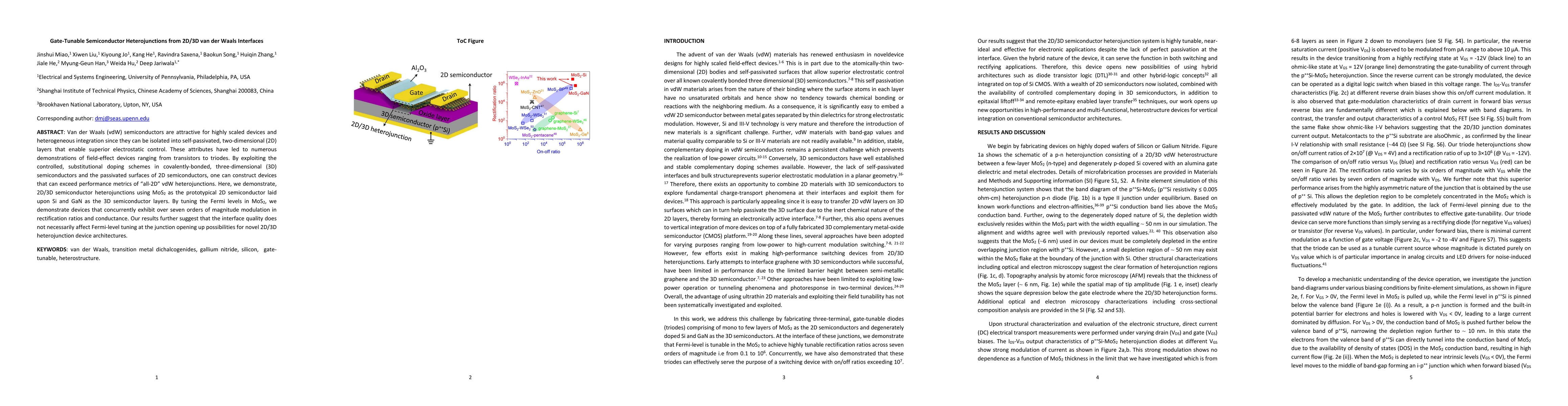
Van der Waals (vdW) semiconductors are attractive for highly scaled devices and heterogeneous integration since they can be isolated into self-passivated, two-dimensional (2D) layers that enable superior electrostatic control. These attributes have led to numerous demonstrations of field-effect devices ranging from transistors to triodes. By exploiting the controlled, substitutional doping schemes in covalently-bonded, three-dimensional (3D) semiconductors and the passivated surfaces of 2D semiconductors, one can construct devices that can exceed performance metrics of 'all-2D' vdW heterojunctions. Here, we demonstrate, 2D/3D semiconductor heterojunctions using MoS2 as the prototypical 2D semiconductor laid upon Si and GaN as the 3D semiconductor layers. By tuning the Fermi levels in MoS2, we demonstrate devices that concurrently exhibit over seven orders of magnitude modulation in rectification ratios and conductance. Our results further suggest that the interface quality does not necessarily affect Fermi-level tuning at the junction opening up possibilities for novel 2D/3D heterojunction device architectures.
AI Key Findings
Get AI-generated insights about this paper's methodology, results, significance, and more — seven facets brought into focus.
Impact
Paper Details
Authors
PDF Preview
Key Terms
Citation Network
Current paper (gray), citations (green), references (blue)
Display is limited for performance on very large graphs.
Discussion 0