Gate-tunable spatial modulation of localized plasmon resonances
Publication
Metrics
AI Quick Summary
This paper demonstrates electrically tunable localized plasmon resonances in semiconductor nanowires by strategically doping the nanowire to achieve localization effects. The study shows that spatial modulation of these resonances can be achieved via field-effect carrier modulation, opening possibilities for electrically tunable plasmonic circuits.
Paper Preview
Abstract
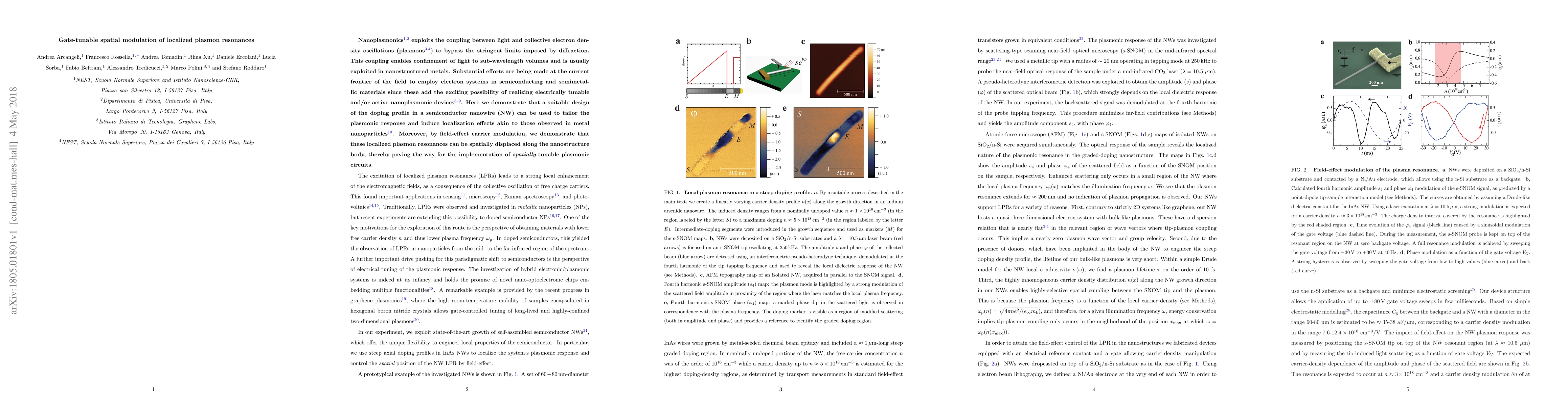
Nanoplasmonics exploits the coupling between light and collective electron density oscillations (plasmons) to bypass the stringent limits imposed by diffraction. This coupling enables confinement of light to sub-wavelength volumes and is usually exploited in nanostructured metals. Substantial efforts are being made at the current frontier of the field to employ electron systems in semiconducting and semimetallic materials since these add the exciting possibility of realizing electrically tunable and/or active nanoplasmonic devices. Here we demonstrate that a suitable design of the doping profile in a semiconductor nanowire (NW) can be used to tailor the plasmonic response and induce localization effects akin to those observed in metal nanoparticles. Moreover, by field-effect carrier modulation, we demonstrate that these localized plasmon resonances can be spatially displaced along the nanostructure body, thereby paving the way for the implementation of spatially tunable plasmonic circuits.
AI Key Findings
Get AI-generated insights about this paper's methodology, results, significance, and more — seven facets brought into focus.
Impact
Paper Details
PDF Preview
Key Terms
Citation Network
Current paper (gray), citations (green), references (blue)
Display is limited for performance on very large graphs.
Discussion 0