Publication
Metrics
AI Quick Summary
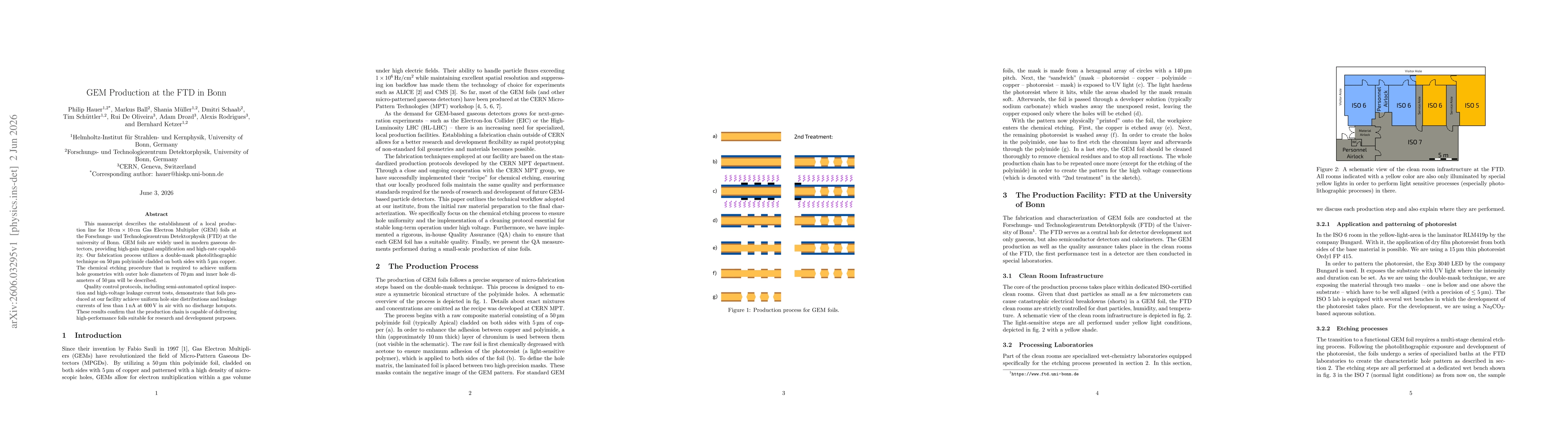
The paper reports the setup of a local 10 cm x 10 cm GEM foil production line at the Bonn FTD, using a 50 μm polyimide substrate with 5 μm copper and a double-mask photolithography process to create 70 μm outer and 50 μm inner hole diameters. Quality checks show uniform hole sizes and very low leakage currents (<1 nA at 600 V in air), indicating reliable, high-performance foils for research and development.
Paper Preview
Abstract
This manuscript describes the establishment of a local production line for 10 cm x 10 cm Gas Electron Multiplier (GEM) foils at the Forschungs- und Technologiezentrum Detektorphysik (FTD) at the university of Bonn. GEM foils are widely used in modern gaseous detectors, providing high-gain signal amplification and high-rate capability. Our fabrication process utilizes a double-mask photolithographic technique on 50 $μ$m polyimide cladded on both sides with 5 $μ$m copper. The chemical etching procedure that is required to achieve uniform hole geometries with outer hole diameters of 70 $μ$m and inner hole diameters of 50 $μ$m will be described. Quality control protocols, including semi-automated optical inspection and high-voltage leakage current tests, demonstrate that foils produced at our facility achieve uniform hole size distributions and leakage currents of less than 1 nA at 600 V in air with no discharge hotspots. These results confirm that the production chain is capable of delivering high-performance foils suitable for research and development purposes.
AI Key Findings
Get AI-generated insights about this paper's methodology, results, significance, and more — seven facets brought into focus.
Discussion 0