Publication
Metrics
AI Quick Summary
This paper proposes a CMOS-compatible method to generate localized strain gradients on Si/SiOx substrates using a SiN passivation layer, which alters the magnetic anisotropy of ferromagnetic materials via magnetoelastic interactions. The method enables the creation of pinning sites for vortex walls in magnetic nanowires, demonstrating substantial pinning fields up to 15 mT, and enabling the development of a power-on magnetic sensor without requiring piezoelectric substrates or high-resolution lithography.
Paper Preview
Abstract
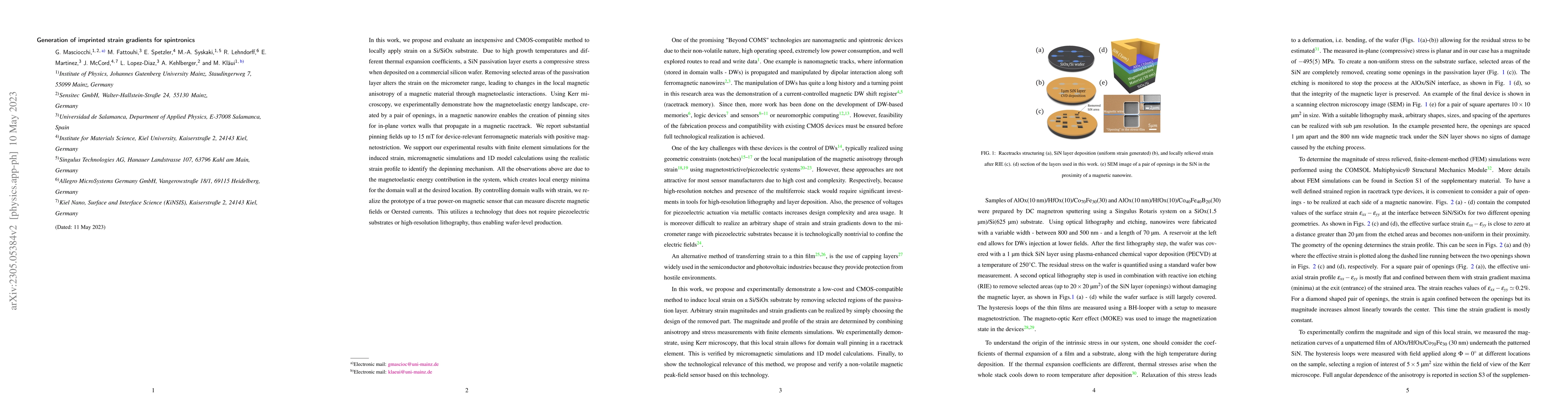
In this work, we propose and evaluate an inexpensive and CMOS-compatible method to locally apply strain on a Si/SiOx substrate. Due to high growth temperatures and different thermal expansion coefficients, a SiN passivation layer exerts a compressive stress when deposited on a commercial silicon wafer. Removing selected areas of the passivation layer alters the strain on the micrometer range, leading to changes in the local magnetic anisotropy of a magnetic material through magnetoelastic interactions. Using Kerr microscopy, we experimentally demonstrate how the magnetoelastic energy landscape, created by a pair of openings, in a magnetic nanowire enables the creation of pinning sites for in-plane vortex walls that propagate in a magnetic racetrack. We report substantial pinning fields up to 15 mT for device-relevant ferromagnetic materials with positive magnetostriction. We support our experimental results with finite element simulations for the induced strain, micromagnetic simulations and 1D model calculations using the realistic strain profile to identify the depinning mechanism. All the observations above are due to the magnetoelastic energy contribution in the system, which creates local energy minima for the domain wall at the desired location. By controlling domain walls with strain, we realize the prototype of a true power-on magnetic sensor that can measure discrete magnetic fields or Oersted currents. This utilizes a technology that does not require piezoelectric substrates or high-resolution lithography, thus enabling wafer-level production.
AI Key Findings
Get AI-generated insights about this paper's methodology, results, significance, and more — seven facets brought into focus.
Impact
Paper Details
Authors
PDF Preview
Key Terms
Citation Network
Current paper (gray), citations (green), references (blue)
Display is limited for performance on very large graphs.
Discussion 0