GeSn Defects and their Impact on Optoelectronic Properties: A Review
Publication
Metrics
AI Quick Summary
This review examines the state-of-the-art in GeSn semiconductor fabrication and discusses the critical role of material defects, such as point and linear defects, on optoelectronic properties, including doping, carrier lifetime, and mobility. It highlights remaining challenges that hinder GeSn's commercialization for applications like LiDARs and lasers.
Paper Preview
Abstract
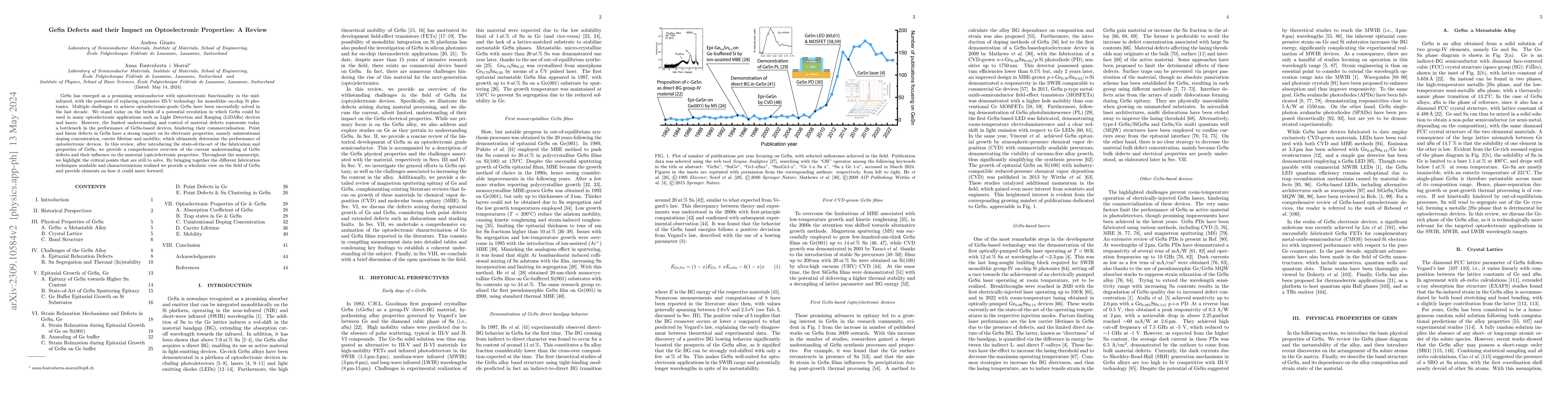
GeSn has emerged as a promising semiconductor with optoelectronic functionality in the mid-infrared, with the potential of replacing expensive III-V technology for monolithic on-chip Si photonics. Multiple challenges to achieve optoelectronic-grade GeSn have been successfully solved in the last decade. We stand today on the brink of a potential revolution in which GeSn could be used in many optoelectronic applications such as Light Detection and Ranging (LiDARs) devices and lasers. However, the limited understanding and control of material defects represents today a bottleneck in the performance of GeSn-based devices, hindering their commercialisation. Point and linear defects in GeSn have a strong impact on its electronic properties, namely unintentional doping concentration, carrier lifetime and mobility, which ultimately determine the performance of optoelectronic devices. In this review, after introducing the state-of-the-art of the fabrication and properties of GeSn, we provide a comprehensive overview of the current understanding of GeSn defects and their influence on the material (opto)electronic properties. Throughout the manuscript, we highlight the critical points that are still to solve. By bringing together the different fabrication techniques available and characterizations realized we provide a wholistic view on the field of GeSn and provide elements on how it could move forward.
AI Key Findings
Get AI-generated insights about this paper's methodology, results, significance, and more — seven facets brought into focus.
Impact
Paper Details
Authors
PDF Preview
Key Terms
Citation Network
Current paper (gray), citations (green), references (blue)
Display is limited for performance on very large graphs.
Discussion 0