Going beyond copper: wafer-scale synthesis of graphene on sapphire
Publication
Metrics
AI Quick Summary
This paper details a metal-free method for growing high-quality monolayer graphene on c-plane sapphire substrates using CVD, identifying the Al-rich reconstruction root31R9 of sapphire as key. The process yields graphene with mobilities above 2000 cm²/Vs and scales to 4-inch and 6-inch wafer sizes with metal contamination suitable for BEOL integration.
Paper Preview
Abstract
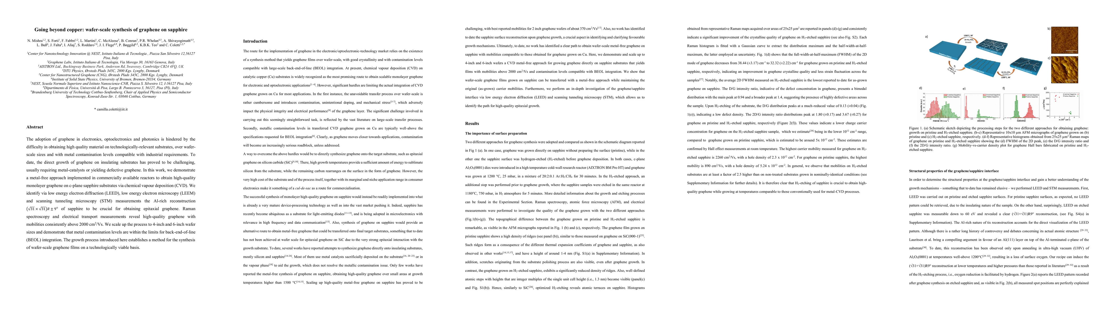
The adoption of graphene in electronics, optoelectronics and photonics is hindered by the difficulty in obtaining high quality material on technologically-relevant substrates, over wafer-scale sizes and with metal contamination levels compatible with industrial requirements. To date, the direct growth of graphene on insulating substrates has proved to be challenging, usually requiring metal-catalysts or yielding defective graphene. In this work, we demonstrate a metal-free approach implemented in commercially available reactors to obtain high-quality monolayer graphene on c-plane sapphire substrates via chemical vapour deposition (CVD). We identify via low energy electron diffraction (LEED), low energy electron microscopy (LEEM) and scanning tunneling microscopy (STM) measurements the Al-rich reconstruction root31R9 of sapphire to be crucial for obtaining epitaxial graphene. Raman spectroscopy and electrical transport measurements reveal high-quality graphene with mobilities consistently above 2000 cm2/Vs. We scale up the process to 4-inch and 6-inch wafer sizes and demonstrate that metal contamination levels are within the limits for back-end-of-line (BEOL) integration. The growth process introduced here establishes a method for the synthesis of wafer-scale graphene films on a technologically viable basis.
AI Key Findings
Get AI-generated insights about this paper's methodology, results, significance, and more — seven facets brought into focus.
Impact
Paper Details
Authors
PDF Preview
Key Terms
Citation Network
Current paper (gray), citations (green), references (blue)
Display is limited for performance on very large graphs.
Discussion 0