Grain boundary strain localization in CdTe solar cell revealed by Scanning 3D X-ray diffraction microscopy
Publication
Metrics
AI Quick Summary
This study uses scanning 3D X-ray diffraction microscopy to map grain boundaries, phase, orientation, and local strain in CdTe solar cells, revealing that high-strain regions are primarily associated with high misorientation grain boundaries, which form a continuous pathway connected to the CdS layer, suggesting sulfur diffusion along these boundaries.
Paper Preview
Abstract
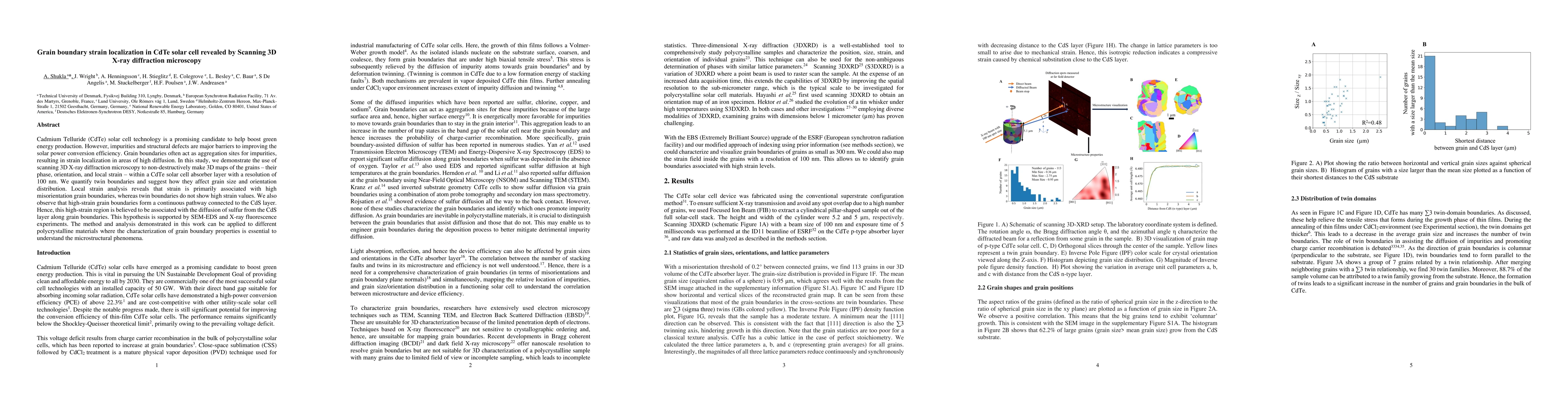
Cadmium Telluride (CdTe) solar cell technology is a promising candidate to help boost green energy production. However, impurities and structural defects are major barriers to improving the solar power conversion efficiency. Grain boundaries often act as aggregation sites for impurities, resulting in strain localization in areas of high diffusion. In this study, we demonstrate the use of scanning 3D X-ray diffraction microscopy to non-destructively make 3D maps of the grains, their phase, orientation, and local strain within a CdTe solar cell absorber layer with a resolution of 100 nm. We quantify twin boundaries and suggest how they affect grain size and orientation distribution. Local strain analysis reveals that strain is primarily associated with high misorientation grain boundaries, whereas twin boundaries do not show high strain values. We also observe that high-strain grain boundaries form a continuous pathway connected to the CdS layer. Hence, this high-strain region is believed to be associated with the diffusion of sulfur from the CdS layer along grain boundaries. This hypothesis is supported by SEM EDS and X-ray fluorescence experiments. The method and analysis demonstrated in this work can be applied to different polycrystalline materials where the characterization of grain boundary properties is essential to understand the microstructural phenomena.
AI Key Findings
Get AI-generated insights about this paper's methodology, results, significance, and more — seven facets brought into focus.
Impact
Paper Details
Authors
PDF Preview
Key Terms
Citation Network
Current paper (gray), citations (green), references (blue)
Display is limited for performance on very large graphs.
Discussion 0