ArxivLens

Quick Summary:

Researchers developed a method for forming high-quality graphene layers on both C and Si faces of semi-insulating 4H- and 6H-SiC substrates using chemical vapor deposition, confirmed by Raman spectroscopy. The process included H2 etching to create surface steps, modifying the substrate morphology and achieving comparable Hall Effect measurements to recent reports.

Journal Reference: Mater. Sci. Forum 615-617, 211 (2009)
DOI: 10.4028/www.scientific.net/MSF.615-617.211
arXiv Id: 0907.5028
Comments: European Conference on Silicon Carbide and Related Materials 2008 (ECSCRM '08), 4 pages, 4 figures
Date Published: 2012-08-27
Date Updated: 2012-08-27

Key Terms (TF-IDF):

graphene (0.303)
morphology (0.253)
face (0.237)
nm (0.232)
substrates (0.226)
faces (0.213)
si (0.200)
axis (0.185)
steps (0.178)
square (0.171)
area (0.163)
samples (0.161)
developed (0.140)
formation (0.139)
insulating (0.135)
raman (0.133)
hall effect (0.132)
commercial (0.131)
sheet (0.131)
concentrations (0.129)
License: http://arxiv.org/licenses/nonexclusive-distrib/1.0/

Summary:

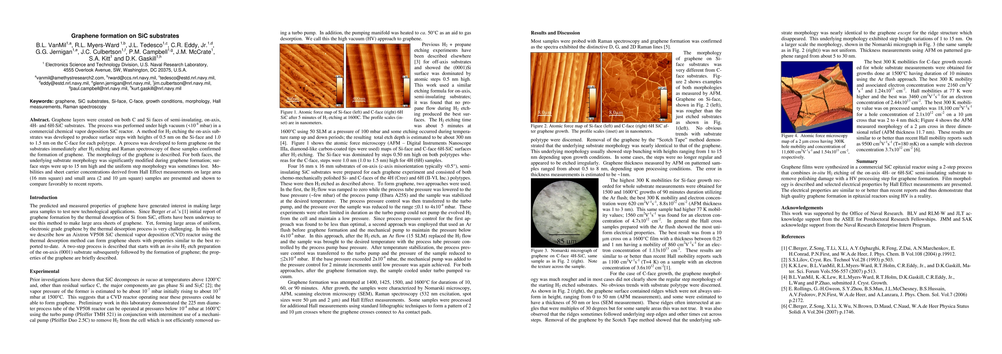
Graphene layers were created on both C and Si faces of semi-insulating, on-axis, 4H- and 6H-SiC substrates. The process was performed under high vacuum (<10-4 mbar) in a commercial chemical vapor deposition SiC reactor. A method for H2 etching the on-axis sub-strates was developed to produce surface steps with heights of 0.5 nm on the Si-face and 1.0 to 1.5 nm on the C-face for each polytype. A process was developed to form graphene on the substrates immediately after H2 etching and Raman spectroscopy of these samples confirmed the formation of graphene. The morphology of the graphene is described. For both faces, the underlying substrate morphology was significantly modified during graphene formation; sur-face steps were up to 15 nm high and the uniform step morphology was sometimes lost. Mo-bilities and sheet carrier concentrations derived from Hall Effect measurements on large area (16 mm square) and small area (2 and 10 um square) samples are presented and shown to compare favorably to recent reports.

Citation & Reference Network Visualization

This graph shows how this paper is connected to other research. The current paper is shown in dark gray, papers that cite it are in green, and papers it references are in blue. You can:

Current Paper
Papers citing this work (Citations)
Papers cited by this work (References)

• Hover over any node to see the paper title

• Click a node to view that paper's details

• Drag nodes to rearrange the graph

• Use the zoom controls (bottom right) to zoom in/out

Citations and References

Title Authors Year Actions
Annealing, design and long-term operation of graphite crucibles for the growth of epitaxial graphene on SiC
M. Shestopalov, Veronika Stará, M. Rejhon, J. Kunc
2024
View Paper
Ultrafine Si evaporation control technology to inhibit the island nucleation of epitaxial graphene on SiC (000-1)
Fengqian Zhu, Yuping Jia, Xiaojuan Sun, Yang Chen, Zhiming Shi, Shunpeng Lv, Mingrui Liu, Ke Jiang, Feng Zhang, Tong Wu, Dabing Li
2024
View Paper
Scanning probe analysis of twisted graphene grown on a graphene/silicon carbide template
Yao Yao, R. Negishi, D. Takajo, M. Takamura, Y. Taniyasu, Yoshihiro Kobayashi
2021
View Paper
Deposition of Tetracoordinate Co(II) Complex with Chalcone Ligands on Graphene
J. Hrubý, Sárka Vavrecková, Lukáš Masaryk, A. Sojka, Jorge Navarro-Giraldo, M. Bartoš, R. Herchel, J. Moncol’, Ivan Nemec, P. Neugebauer
2020
View Paper
Van der Waals Epitaxy of III‐Nitride Semiconductors Based on 2D Materials for Flexible Applications
Jiadong Yu, Lai Wang, Z. Hao, Yi Luo, Changzheng Sun, Jian Wang, Yanjun Han, B. Xiong, Hongtao Li
2019
View Paper
A graphene-based hybrid material with quantum bits prepared by the double Langmuir–Schaefer method
J. Hrubý, V. Santana, D. Kostiuk, Martin Bouček, S. Lenz, M. Kern, P. Šiffalovič, J. van Slageren, P. Neugebauer
2019
View Paper
Multi-scale investigation of interface properties, stacking order and decoupling of few layer graphene on C-face 4H-SiC
C. Bouhafs, A. Zakharov, I. Ivanov, F. Giannazzo, J. Eriksson, V. Stanishev, P. Kühne, T. Iakimov, T. Hofmann, M. Schubert, F. Roccaforte, R. Yakimova, V. Darakchieva
2017
View Paper
Planar nanosized field emission cathodes on the basis of graphene/semi-insulating silicon carbide fabricated by focused ion beam
L. Jityaev, O. A. Ageev, A. M. Svetlichnyi, A. S. Kolomiytsev, O. Spiridonov
2016
View Paper
Analysis of Heat Dissipation of Epitaxial Graphene Devices on SiC
Kangmu Lee, J. Moon, T. Oh, S. Kim, P. Asbeck
2014
View Paper
Mode-locked 2-μm wavelength fiber laser using a graphene-saturable absorber
M. Currie, T. Anderson, V. Wheeler, L. Nyakiti, Nelson Y. Garces, R. Myers-Ward, Charles R. Eddy, F. Kub, D. Gaskill
2013
View Paper
Epitaxial Growth of III–Nitride/Graphene Heterostructures for Electronic Devices
N. Nepal, V. Wheeler, T. Anderson, F. Kub, M. Mastro, R. Myers-Ward, S. Qadri, J. Freitas, S. Hernández, L. Nyakiti, S. Walton, K. Gaskill, C. Jr.
2013
View Paper
Local solid phase growth of few-layer graphene on silicon carbide from nickel silicide supersaturated with carbon
E. Escobedo-Cousin, K. Vassilevski, T. Hopf, N. Wright, A. O'Neill, A. Horsfall, J. Goss, P. Cumpson
2013
View Paper
Enabling graphene-based technologies: Toward wafer-scale production of epitaxial graphene
L. Nyakiti, Virginia D. Wheeler, N. Garces, R. Myers-Ward, C. Eddy, D. Gaskill
2012
View Paper
Visible to vacuum ultraviolet dielectric functions of epitaxial graphene on 3C and 4H SiC polytypes determined by spectroscopic ellipsometry
A. Boosalis, T. Hofmann, V. Darakchieva, R. Yakimova, M. Schubert
2012
View Paper
Fluorine functionalization of epitaxial graphene for uniform deposition of thin high-κ dielectrics
V. Wheeler, Nelson Y. Garces, L. Nyakiti, R. Myers-Ward, G. Jernigan, J. Culbertson, C. Eddy, D. Kurt Gaskill
2012
View Paper
Bilayer graphene grown on 4H-SiC (0001) step-free mesas.
L. Nyakiti, R. Myers-Ward, Virginia D. Wheeler, E. Imhoff, F. Bezares, Hayden Chun, Joshua D. Caldwell, Adam L Friedman, B. Matis, Jeffrey W. Baldwin, Paul M. Campbell, J. Culbertson, C. Eddy, G. Jernigan, D. Gaskill
2012
View Paper
Epitaxial Growth of Graphene and Their Applications in Devices
Ti-Yu Lin
2011
View Paper
Carbide‐Derived Carbons – From Porous Networks to Nanotubes and Graphene
V. Presser, Min Heon, Y. Gogotsi
2011
View Paper
Growth of 4H- and 3C-SiC Epitaxial Layers on 4H-SiC Step-Free Mesas
R. Myers-Ward, L. Nyakiti, J. Hite, O. Glembocki, F. Bezares, J. Caldwell, E. Imhoff, K. Hobart, J. Culbertson, Y. Picard, V. Wheeler, C. Eddy, D. Gaskill
2011
View Paper
Probing residual strain in epitaxial graphene layers on 4H-SiC(0001¯) with Raman spectroscopy
A. Strudwick, G. Creeth, N. Johansson, C. Marrows
2011
View Paper
Morphology characterization of argon-mediated epitaxial graphene on C-face SiC
J. Tedesco, G. Jernigan, J. Culbertson, J. Hite, Yang Yang, K. Daniels, R. Myers-Ward, C. Eddy, Jr., J. Robinson, K. Trumbull, Maxwell T. Wetherington, P. Campbell, D. Gaskill
2010
View Paper
GHz devices from epitaxial graphene on SiC
D.K. Gaskilla, J. Moon, J. Tedesco, J. Robinson, A. Friedman, P. Campbell, G. Jernigan, J. Hite, R. Myers-Ward, C. Eddy, M. Fanton
2009
View Paper
Techniques for the Dry Transfer of Epitaxial Graphene onto Arbitrary Substrates
Joshua D. Caldwell, T. Anderson, K. Hobart, J. Culbertson, G. Jernigan, F. Kub, J. Tedesco, J. Hite, M. Mastro, R. Myers-Ward, Charles R. Eddy, Paul M. Campbell, D. Gaskill
2009
View Paper
Hall effect mobility of epitaxial graphene grown on silicon carbide
J. Tedesco, B. Vanmil, R. Myers-Ward, J. Mccrate, S. Kitt, P. Campbell, G. Jernigan, J. Culbertson, C. Eddy, Jr., D. Gaskill
2009
View Paper
Correlating Raman spectral signatures with carrier mobility in epitaxial graphene: a guide to achieving high mobility on the wafer scale.
J. Robinson, Maxwell T. Wetherington, J. Tedesco, P. Campbell, X. Weng, J. Stitt, M. Fanton, E. Frantz, D. Snyder, B. Vanmil, G. Jernigan, R. Myers-Ward, C. Eddy, D. Gaskill
2009
View Paper
Extreme Epitaxial Growth of III-N Semiconductor Thin Films
D. Pennachio
2019
View Paper
Synthesis, Structure, and Properties of Graphene and Graphene Oxide
Q. Zheng, Jang‐Kyo Kim
2015
View Paper
Challenges to graphene growth on SiC(0 0 0 1‾): Substrate effects, hydrogen etching and growth ambient
Z. Robinson, G. Jernigan, M. Currie, J. Hite, K. Bussmann, L. Nyakiti, N. Garces, A. Nath, M. V. Rao, V. Wheeler, R. Myers-Ward, J. Wollmershauser, B. Feigelson, C. Eddy, D. K. Gaskill
2015
View Paper
Atomic Layer Deposition of Dielectrics on Graphene
N. Garces, V. Wheeler, D. K. Gaskill
2012
View Paper
Study on the Possibility of Graphene Growth on 4H-Silicon Carbide Surfaces via Laser Processing
D. Perrone, G. Maccioni, A. Chiolerio, C. M. D. Marigorta, M. Naretto, P. Pandolfi, P. Martino, C. Ricciardi, A. Chiodoni, E. Celasco, L. Scaltrito, S. Ferrero
2009
View Paper

Comments (0)

This website uses cookies to ensure you get the best experience. Learn more