Graphene Heterostructure-Based Non-Volatile Memory Devices with Top Floating Gate Programming
Publication
Metrics
Paper Preview
Abstract
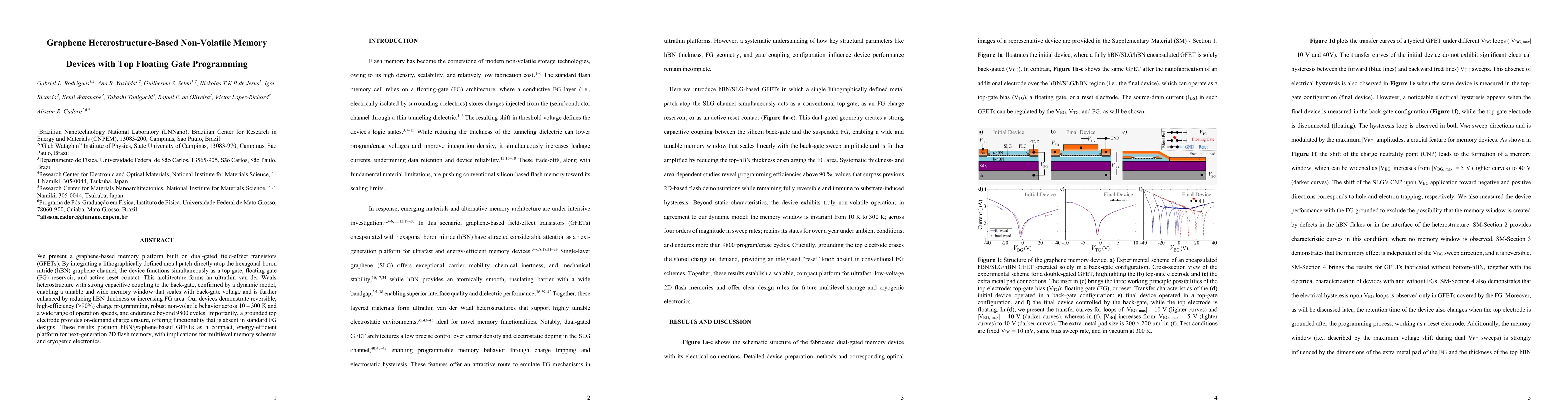
We present a graphene-based memory platform built on dual-gated field-effect transistors (GFETs). By integrating a lithographically defined metal patch directly atop the hexagonal boron nitride (hBN)-graphene channel, the device functions simultaneously as a top gate, floating gate (FG) reservoir, and active reset contact. This architecture forms an ultrathin van der Waals heterostructure with strong capacitive coupling to the back-gate, confirmed by a dynamic model, enabling a tunable and wide memory window that scales with back-gate voltage and is further enhanced by reducing hBN thickness or increasing FG area. Our devices demonstrate reversible, high-efficiency charge programming, robust non-volatile behavior across 10 to 300 K and a wide range of operation speeds, and endurance beyond 9800 cycles. Importantly, a grounded top electrode provides on-demand charge erasure, offering functionality that is absent in standard FG designs. These results position hBN/graphene-based GFETs as a compact, energy-efficient platform for next-generation 2D flash memory, with implications for multilevel memory schemes and cryogenic electronics.
AI Key Findings
Get AI-generated insights about this paper's methodology, results, significance, and more — seven facets brought into focus.
Impact
Paper Details
Authors
PDF Preview
Citation Network
Current paper (gray), citations (green), references (blue)
Display is limited for performance on very large graphs.
Discussion 0