01
MethodologyHow they did it
Brief description of the research methodology used
This paper reviews recent advancements in graphene devices supported by hexagonal boron nitride, emphasizing the use of scanning tunneling microscopy and highlighting significant findings from electrical transport measurements, which enhance the understanding of graphene's properties and potential new phenomena.
This paper reviews recent advancements in graphene devices supported by hexagonal boron nitride, emphasizing the use of scanning tunneling microscopy and highlighting significant findings from electrical transport measurements, which enhance the understanding of graphene's properties and potential new phenomena.
Brief description of the research methodology used More in Methodology →
Main finding 1 — Main finding 2 More in Key Results →
Why this research is important and its potential impact More in Significance →
Limitation 1 — Limitation 2 More in Limitations →
The field of graphene research has developed rapidly since its first isolation by mechanical exfoliation in 2004. Due to the relativistic Dirac nature of its charge carriers, graphene is both a promising material for next-generation electronic devices and a convenient low-energy testbed for intrinsically high-energy physical phenomena. Both of these research branches require the facile fabrication of clean graphene devices so as not to obscure its intrinsic physical properties. Hexagonal boron nitride has emerged as a promising substrate for graphene devices, as it is insulating, atomically flat and provides a clean charge environment for the graphene. Additionally, the interaction between graphene and boron nitride provides a path for the study of new physical phenomena not present in bare graphene devices. This review focuses on recent advancements in the study of graphene on hexagonal boron nitride devices from the perspective of scanning tunneling microscopy with highlights of some important results from electrical transport measurements.
Seven facets of this paper, analysed and brought into focus by AI.
Why this research is important and its potential impact
Brief description of the research methodology used
Why this research is important and its potential impact
Main technical or theoretical contribution
What makes this work novel or different from existing research
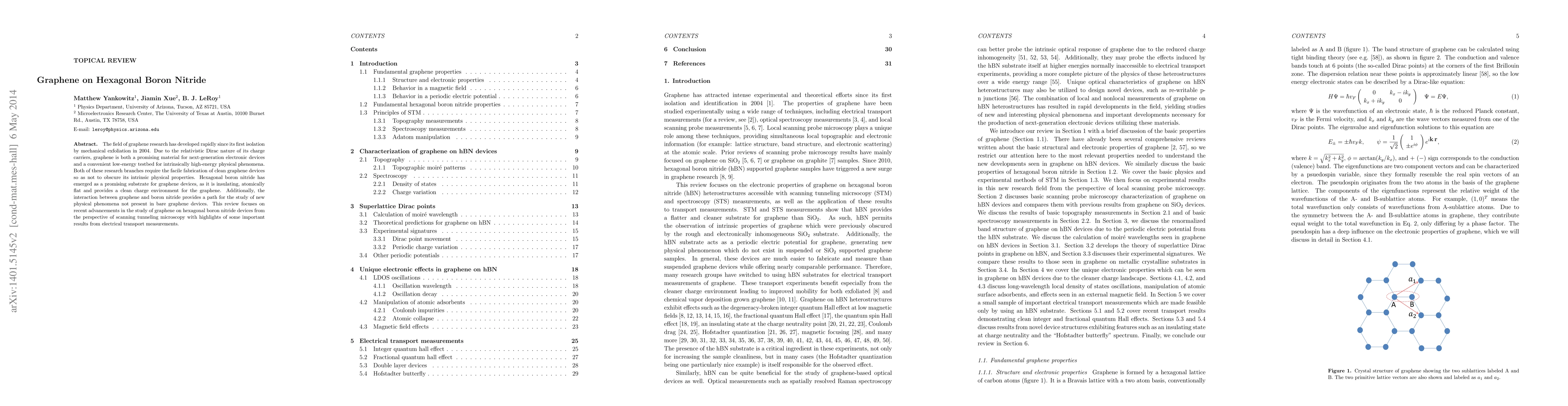
Current paper (gray), citations (green), references (blue)
Display is limited for performance on very large graphs.
Discussion 0