Publication
Metrics
Paper Preview
Abstract
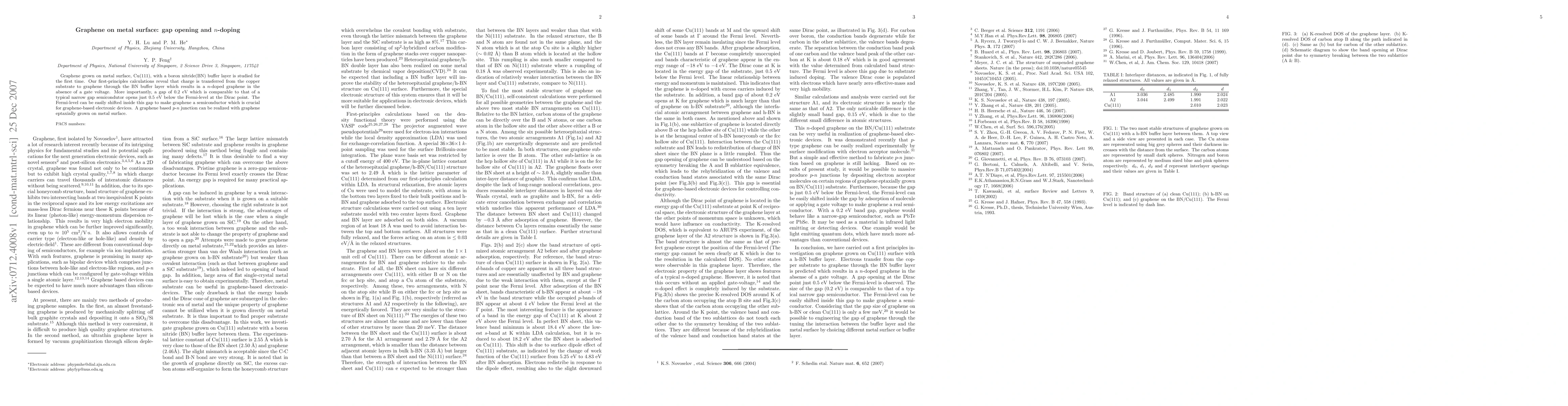
Graphene grown on metal surface, Cu(111), with a boron nitride(BN) buffer layer is studied for the first time. Our first-principles calculations reveal that charge is transferred from the copper substrate to graphene through the BN buffer layer which results in a n-doped graphene in the absence of a gate voltage. More importantly, a gap of 0.2 eV which is comparable to that of a typical narrow gap semicondutor opens just 0.5 eV below the Fermi-level at the Dirac point. The Fermi-level can be easily shifted inside this gap to make graphene a semiconductor which is crucial for graphene-based electronic devices. A graphene based p-n junction can be realized with graphene eptaxially grown on metal surface.
AI Key Findings
Get AI-generated insights about this paper's methodology, results, significance, and more — seven facets brought into focus.
Impact
Paper Details
PDF Preview
Key Terms
Citation Network
Current paper (gray), citations (green), references (blue)
Display is limited for performance on very large graphs.
Discussion 0