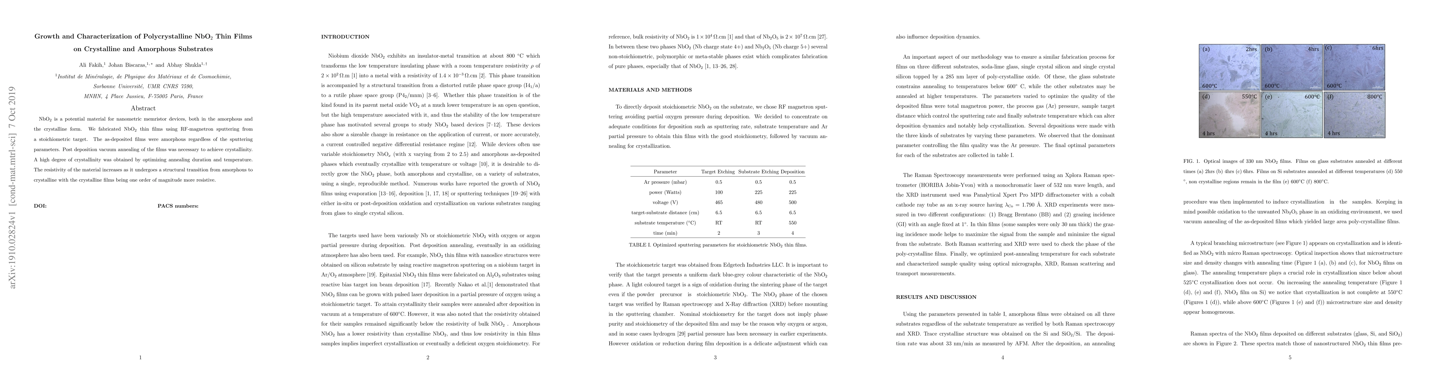
Summary
NbO2 is a potential material for nanometric memristor devices, both in the amorphous and the crystalline form. We fabricated NbO2 thin films using RF-magnetron sputtering from a stoichiometric target. The as-deposited films were amorphous regardless of the sputtering parameters. Post deposition vacuum annealing of the films was necessary to achieve crystallinity. A high degree of crystallinity was obtained by optimizing annealing duration and temperature. The resistivity of the material increases as it undergoes a structural transition from amorphous to crystalline with the crystalline films being one order of magnitude more resistive.
AI Key Findings
Get AI-generated insights about this paper's methodology, results, and significance.
Paper Details
PDF Preview
Key Terms
Citation Network
Current paper (gray), citations (green), references (blue)
Display is limited for performance on very large graphs.
Similar Papers
Found 4 papersPreparation, characterization, and electrical properties of epitaxial NbO2 thin film lateral devices
Elastic Modulus of Polycrystalline Halide Perovskite Thin Films on Substrates
Brian W. Sheldon, Madhuja Layek, In Seok Yang et al.
| Title | Authors | Year | Actions |
|---|
Comments (0)