High Current Density Vertical Tunneling Transistors from Graphene/Highly-Doped Silicon Heterostructures
Publication
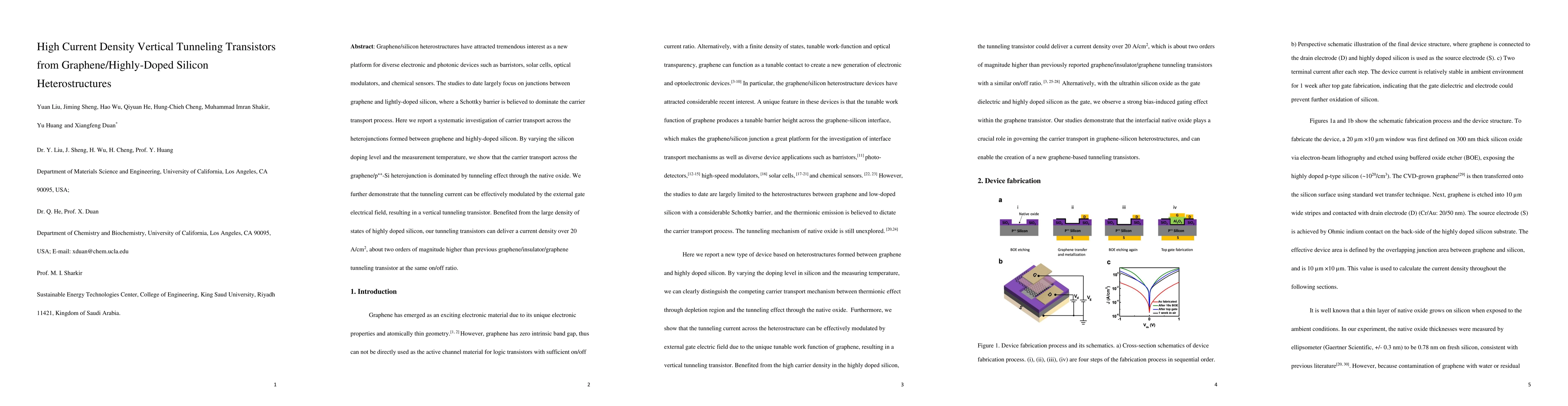
Metrics
AI Quick Summary
This study investigates carrier transport across graphene/highly-doped silicon heterojunctions, showing that tunneling through the native oxide dominates the process. It demonstrates a vertical tunneling transistor with current densities over 20 A/cm², significantly higher than previous graphene-based transistors.
Paper Preview
Abstract
Graphene/silicon heterostructures have attracted tremendous interest as a new platform for diverse electronic and photonic devices such as barristors, solar cells, optical modulators, and chemical sensors. The studies to date largely focus on junctions between graphene and lightly-doped silicon, where a Schottky barrier is believed to dominate the carrier transport process. Here we report a systematic investigation of carrier transport across the heterojunctions formed between graphene and highly-doped silicon. By varying the silicon doping level and the measurement temperature, we show that the carrier transport across the graphene/p++-Si heterojunction is dominated by tunneling effect through the native oxide. We further demonstrate that the tunneling current can be effectively modulated by the external gate electrical field, resulting in a vertical tunneling transistor. Benefited from the large density of states of highly doped silicon, our tunneling transistors can deliver a current density over 20 A/cm2, about two orders of magnitude higher than previous graphene/insulator/graphene tunneling transistor at the same on/off ratio.
AI Key Findings — Failed
Key findings generation failed. Failed to start generation process
Impact
Paper Details
PDF Preview
Key Terms
Citation Network
Current paper (gray), citations (green), references (blue)
Display is limited for performance on very large graphs.
Discussion 0