01
MethodologyHow they did it
Brief description of the research methodology used
This paper proposes a novel scheme for vertical coupling between silicon nitride waveguides on glass and silicon waveguides on insulator, using overlapping inverse double tapers. Simulation results show low insertion losses and high alignment tolerances, indicating the potential for high-density, passive assembly in co-packaged optics designs.
Brief description of the research methodology used More in Methodology →
Main finding 1 — Main finding 2 More in Key Results →
Why this research is important and its potential impact More in Significance →
Limitation 1 — Limitation 2 More in Limitations →
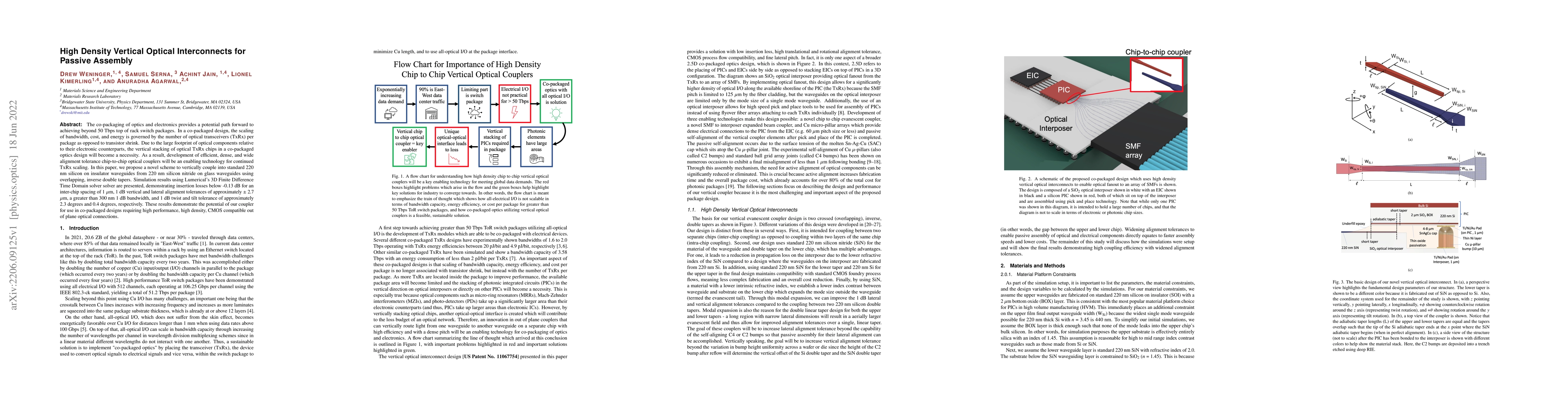
The co-packaging of optics and electronics provides a potential path forward to achieving beyond 50 Tbps top of rack switch packages. In a co-packaged design, the scaling of bandwidth, cost, and energy is governed by the number of optical transceivers (TxRx) per package as opposed to transistor shrink. Due to the large footprint of optical components relative to their electronic counterparts, the vertical stacking of optical TxRx chips in a co-packaged optics design will become a necessity. As a result, development of efficient, dense, and wide alignment tolerance chip-to-chip optical couplers will be an enabling technology for continued TxRx scaling. In this paper, we propose a novel scheme to vertically couple into standard 220 nm silicon on insulator waveguides from 220 nm silicon nitride on glass waveguides using overlapping, inverse double tapers. Simulation results using Lumerical's 3D Finite Difference Time Domain solver solver are presented, demonstrating insertion losses below -0.13 dB for an inter-chip spacing of 1 $\mu$m, 1 dB vertical and lateral alignment tolerances of approximately $\pm$ 2.7 $\mu$m, a greater than 300 nm 1 dB bandwidth, and 1 dB twist and tilt tolerance of approximately 2.3 degrees and 0.4 degrees, respectively. These results demonstrate the potential of our coupler for use in co-packaged designs requiring high performance, high density, CMOS compatible out of plane optical connections.
Seven facets of this paper, analysed and brought into focus by AI.
Why this research is important and its potential impact
Brief description of the research methodology used
Why this research is important and its potential impact
Main technical or theoretical contribution
What makes this work novel or different from existing research
Current paper (gray), citations (green), references (blue)
Display is limited for performance on very large graphs.
Discussion 0