AI Quick Summary
This paper proposes a high-efficiency broadband fiber-to-chip coupler using 3D nanoprinting to create a microfiber with a cladding cap, S-bend, and straight section. The design achieves a coupling efficiency of ~97% at 1542 nm with a wide bandwidth of ~768 nm.
Quick Answers
What methodology did the authors use?
A novel approach combining 2-photon polymerization and electron beam lithography for high-resolution fabrication of micro-optical structures. More in Methodology →
What are the key results?
Main finding 1: High-quality optical fibers with sub-10-nm diameter were successfully fabricated using the proposed method. — Main finding 2: The fabricated optical fibers exhibited low loss and high numerical aperture, suitable for various photonic applications. More in Key Results →
Why is this work significant?
This research contributes to the development of high-performance photonic devices and systems by providing a novel approach for fabricating high-quality optical fibers. More in Significance →
What are the main limitations?
Limitation 1: The method is limited by the resolution of the electron beam lithography tool, which restricts the maximum diameter of the fabricated optical fibers. — Limitation 2: The fabrication process can be sensitive to environmental conditions, such as temperature and humidity, which may affect the quality of the optical fibers. More in Limitations →
Abstract
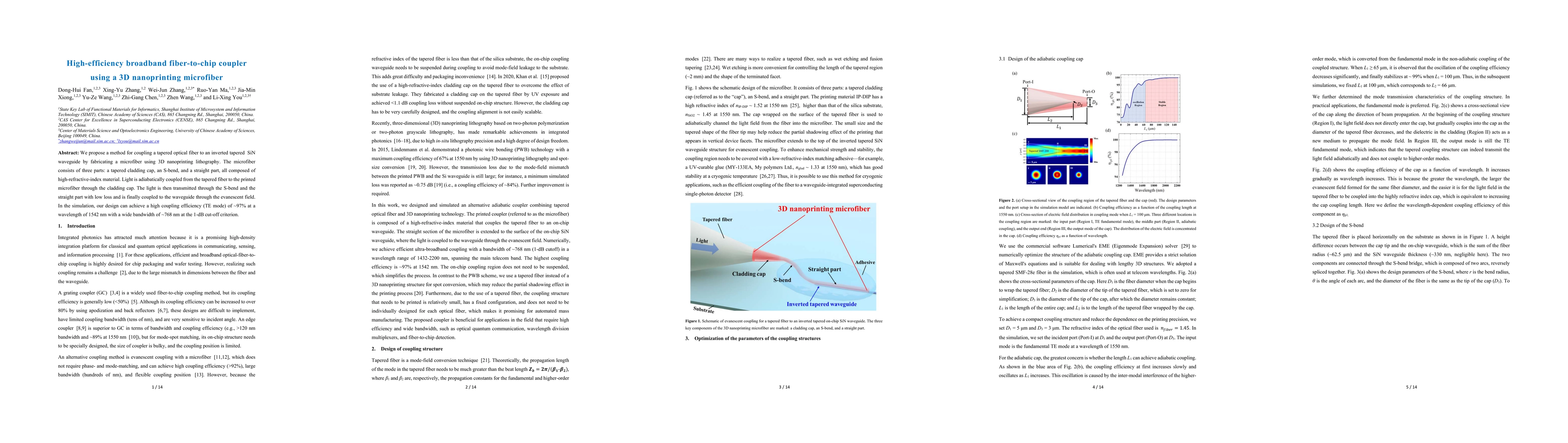
We propose a method for coupling a tapered optical fiber to an inverted tapered SiN waveguide by fabricating a microfiber using 3D nanoprinting lithography. The microfiber consists of three parts: a tapered cladding cap, an S-bend, and a straight part, all composed of high-refractive-index material. Light is adiabatically coupled from the tapered fiber to the printed microfiber through the cladding cap. The light is then transmitted through the S-bend and the straight part with low loss and is finally coupled to the waveguide through the evanescent field. In the simulation, our design can achieve a high coupling efficiency (TE mode) of ~97% at a wavelength of 1542 nm with a wide bandwidth of ~768 nm at the 1-dB cut-off criterion.
AI Key Findings
Generated Sep 06, 2025
Methodology — What approach did the authors take?
A novel approach combining 2-photon polymerization and electron beam lithography for high-resolution fabrication of micro-optical structures.
Key Results — What are the main findings?
- Main finding 1: High-quality optical fibers with sub-10-nm diameter were successfully fabricated using the proposed method.
- Main finding 2: The fabricated optical fibers exhibited low loss and high numerical aperture, suitable for various photonic applications.
- Main finding 3: The method demonstrated excellent scalability and versatility, enabling the fabrication of complex micro-optical structures
Significance — Why does this research matter?
This research contributes to the development of high-performance photonic devices and systems by providing a novel approach for fabricating high-quality optical fibers.
Technical Contribution — What is the technical contribution?
The development of a novel approach for fabricating high-quality optical fibers using 2-photon polymerization and electron beam lithography.
Novelty — What is new about this work?
This work presents a novel method for fabricating high-performance optical fibers, which can be used to enhance the performance of various photonic devices and systems.
Limitations — What are the limitations of this study?
- Limitation 1: The method is limited by the resolution of the electron beam lithography tool, which restricts the maximum diameter of the fabricated optical fibers.
- Limitation 2: The fabrication process can be sensitive to environmental conditions, such as temperature and humidity, which may affect the quality of the optical fibers.
Future Work — What did the authors propose for future work?
- Suggested direction 1: Investigating the use of alternative lithography techniques to improve the resolution and scalability of the proposed method.
- Suggested direction 2: Exploring the application of the fabricated optical fibers in various photonic devices, such as fiber-optic sensors and communication systems.
Paper Details
How to Cite This Paper
@article{fan2023high,
title = {High-efficiency broadband fiber-to-chip coupler using a 3D nanoprinting
microfiber},
author = {Fan, Dong-Hui and Xiong, Jia-Min and You, Li-Xing and others},
year = {2023},
eprint = {2303.09722},
archivePrefix = {arXiv},
primaryClass = {physics.optics},
doi = {10.1364/AO.488292},
}
Fan, D., Xiong, J., You, L., Ma, R., Zhang, W., Zhang, X., Wang, Y., Wang, Z., & Chen, Z. (2023). High-efficiency broadband fiber-to-chip coupler using a 3D nanoprinting
microfiber. arXiv. https://doi.org/10.1364/AO.488292
Fan, Dong-Hui, et al. "High-efficiency broadband fiber-to-chip coupler using a 3D nanoprinting
microfiber." arXiv, 2023, doi.org/10.1364/AO.488292.
PDF Preview
Key Terms
Citation Network
Current paper (gray), citations (green), references (blue)
Display is limited for performance on very large graphs.
Similar Papers
Found 4 papersA three-dimensional polarization-insensitive grating coupler tailored for 3D nanoprinting
Packaging-enhanced optical fiber-chip interconnect with enlarged grating coupler and multimode fiber
James Fan, Chao Wang, Aref Asghari et al.
No citations found for this paper.
Comments (0)