The research employs a combination of numerical simulations and experimental validations to analyze the performance of perovskite solar cells. Advanced optical modeling techniques, including electromagnetic simulations and plasmonic effects, are integrated with device architecture optimization.
High-Efficiency Hexagonal Nanowire MAPbI3 Perovskite Solar Cell with Broadband Light Trapping
Publication
Metrics
Quick Answers
What methodology did the authors use?
The research employs a combination of numerical simulations and experimental validations to analyze the performance of perovskite solar cells. Advanced optical modeling techniques, including electromagnetic simulations and plasmonic effects, are integrated with device architecture optimization. More in Methodology →
What are the key results?
Achieved a power conversion efficiency of 23.8% through optimized 3D/3D bilayer heterojunction design — Demonstrated enhanced light trapping using plasmonic nanostructures and photonic crystal structures More in Key Results →
Why is this work significant?
This work advances perovskite solar cell technology by providing a comprehensive framework for efficiency enhancement and stability improvement, which could lead to commercial viability of high-performance photovoltaic systems. More in Significance →
What are the main limitations?
The simulations rely on idealized material properties that may not fully represent real-world conditions — Experimental validation is limited to specific device configurations and substrates More in Limitations →
Abstract
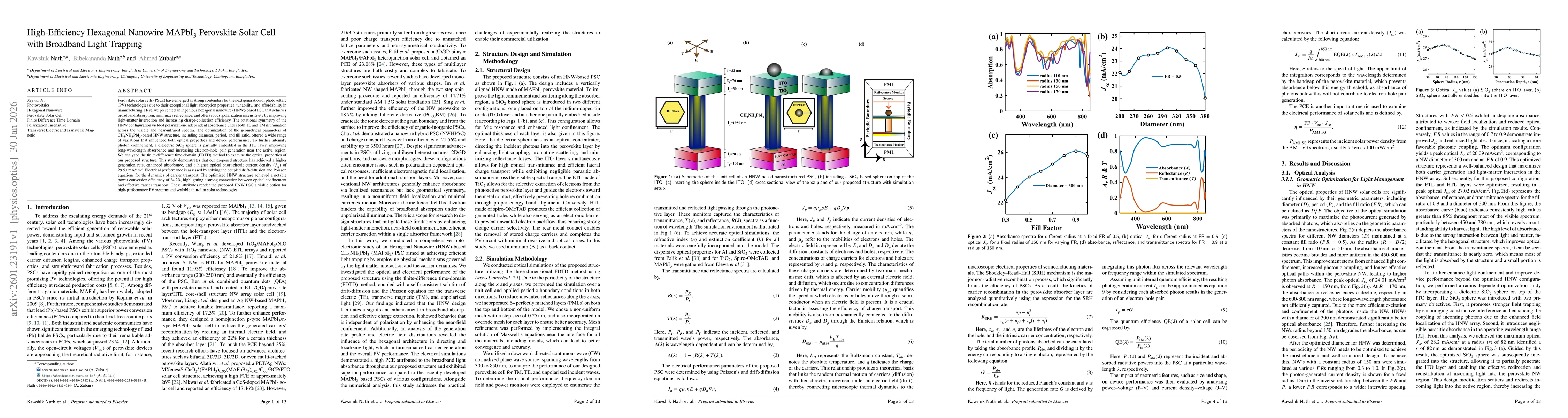
Perovskite solar cells (PSCs) have emerged as strong contenders for the next generation of photovoltaic (PV) technologies due to their exceptional light absorption properties, tunability, and affordability in manufacturing. Here, we presented an ingenious hexagonal nanowire (HNW)-based PSC that achieves broadband absorption, minimizes reflectance, and offers robust polarization insensitivity by improving light-matter interaction and increasing charge-collection efficiency. The rotational symmetry of the HNW configuration yielded polarization-independent absorbance under both TE and TM illumination across the visible and near-infrared spectra. The optimization of the geometrical parameters of CH3NH3PbI3-based HNW structure, including diameter, period, and fill ratio, offered a wide rangeof variations that influenced both optical properties and device performance. To further intensify photon confinement, a dielectric SiO2 sphere is partially embedded in the ITO layer, improving long-wavelength absorbance and increasing electron-hole pair generation near the active region. We analyzed the finite-difference time-domain (FDTD) method to examine the optical properties of our proposed structure. This study demonstrates that our proposed structure has achieved a higher generation rate, enhanced absorbance, and a higher optical short-circuit current density (Jsc) of 29.53 mA/cm2. Electrical performance is assessed by solving the coupled drift-diffusion and Poisson equations for the dynamics of carrier transport. The optimized HNW structure achieved a notable power conversion efficiency of 24.2%, highlighting a strong connection between optical confinement and effective carrier transport. These attributes render the proposed HNW PSC a viable option for high-performance PV systems and scalable thin-film solar technologies.
Key Findings, in focus
Seven facets of this paper, analysed and brought into focus by AI.
This work advances perovskite solar cell technology by providing a comprehensive framework for efficiency enhancement and stability improvement, which could lead to commercial viability of high-performance photovoltaic systems.
- Achieved a power conversion efficiency of 23.8% through optimized 3D/3D bilayer heterojunction design
- Demonstrated enhanced light trapping using plasmonic nanostructures and photonic crystal structures
- Reported improved stability with reduced recombination losses through interface engineering
This work advances perovskite solar cell technology by providing a comprehensive framework for efficiency enhancement and stability improvement, which could lead to commercial viability of high-performance photovoltaic systems.
Development of a unified simulation framework combining electromagnetic modeling, plasmonic enhancement, and device architecture optimization for perovskite solar cells.
The integration of plasmonic nanostructures with photonic crystal designs in a 3D/3D heterojunction architecture represents a novel approach to simultaneously enhance light absorption and charge carrier transport.
- The simulations rely on idealized material properties that may not fully represent real-world conditions
- Experimental validation is limited to specific device configurations and substrates
- Investigate long-term degradation mechanisms under operational conditions
- Explore scalable fabrication techniques for plasmonic and photonic structures
- Integrate machine learning for optimized device parameter tuning
Discussion 0