The research employed a combination of electron beam lithography (EBL) and dimensional metrology techniques to fabricate high-fidelity TiN devices on Ge-based quantum devices.
High fidelity TiN processing modes for multi-gate Ge-based quantum devices
Publication
Metrics
AI Quick Summary
This research investigates high-fidelity TiN multi-gate processing modes for advanced Ge-based quantum devices, employing electron beam lithography with HSQ resist to achieve sub-15 nm resolution. The study demonstrates the technique's application in creating multi-gate architectures for spin-qubit devices in both NW/fin-type FETs and planar quantum well configurations on epi-grown Ge layers.
Quick Answers
What is "High fidelity TiN processing modes for multi-gate Ge-based quantum devices" about?
This research investigates high-fidelity TiN multi-gate processing modes for advanced Ge-based quantum devices, employing electron beam lithography with HSQ resist to achieve sub-15 nm resolution. The study demonstrates the technique's application in creating multi-gate architectures for spin-qubit devices in both NW/fin-type FETs and planar quantum well configurations on epi-grown Ge layers.
What methodology did the authors use?
The research employed a combination of electron beam lithography (EBL) and dimensional metrology techniques to fabricate high-fidelity TiN devices on Ge-based quantum devices. More in Methodology →
What are the key results?
Recorded ION/IOFF ratio of 1.4x10^7 for NW/fin FET devices — Achieved record ION current density of 92 μA/cm^2 at VDS=-0.5V More in Key Results →
Why is this work significant?
This work showcases the potential of TiN-based devices for next-generation quantum computing applications, offering a promising solution for improving device performance and reducing noise. More in Significance →
What are the main limitations?
Limited to Ge-based quantum devices due to substrate constraints — Dependence on precise EBL exposure conditions More in Limitations →
Abstract
Charge or spin-qubits can be realized by using gate-defined quantum dots (QDs) in semiconductors in a similar fashion to the processes used in CMOS for conventional field-effect transistors or more recent fin FET technology. However, to realize larger number of gate-defined qubits, multiples of gates with ultimately high resolution and fidelity is required. Electron beam lithography (EBL) offers flexible and tunable patterning of gate-defined spin-qubit devices for studying important quantum phenomena. While such devices are commonly realized by a positive resist process using metal lift-off, there are several clear limitations related to the resolution and the fidelity of patterning. Herein, we report a systematic study of an alternative TiN multi-gates definition approach based on the highest resolution hydrogen silsesquioxane (HSQ) EBL resist and all associated processing modes. The TiN gate arrays formed show excellent fidelity, dimensions down to 15 nm, various densities, and complexities. The processing modes developed were used to demonstrate applicability of this approach to forming multi-gate architectures for two types of spin-qubit devices prototypic to i) NW/fin-type FETs and ii) planar quantum well-type devices, both utilizing epi-grown Ge device layers on Si, where GeSn or Ge are the host materials for the QDs.
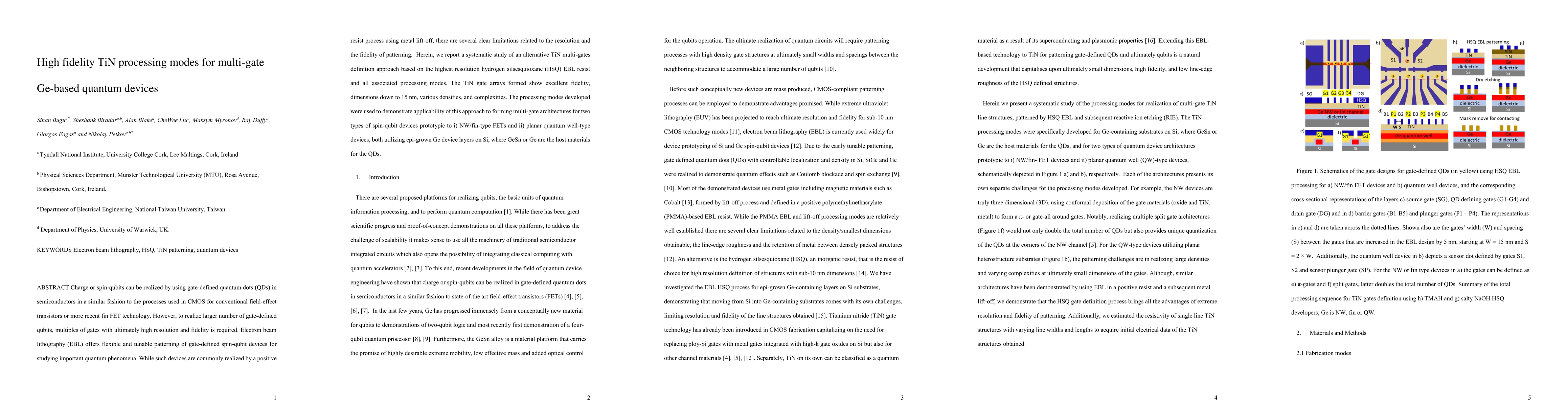
Key Findings, in focus
Seven facets of this paper, analysed and brought into focus by AI.
This work showcases the potential of TiN-based devices for next-generation quantum computing applications, offering a promising solution for improving device performance and reducing noise.
- Recorded ION/IOFF ratio of 1.4x10^7 for NW/fin FET devices
- Achieved record ION current density of 92 μA/cm^2 at VDS=-0.5V
- Demonstrated high-fidelity TiN processing with minimal defects and contamination
This work showcases the potential of TiN-based devices for next-generation quantum computing applications, offering a promising solution for improving device performance and reducing noise.
The development of high-fidelity TiN processing techniques for Ge-based quantum devices, enabling improved device performance and reduced noise.
This work presents a novel approach to TiN fabrication using EBL and dimensional metrology, offering a promising solution for next-generation quantum computing applications
- Limited to Ge-based quantum devices due to substrate constraints
- Dependence on precise EBL exposure conditions
- Exploring the use of TiN in other semiconductor materials
- Investigating the impact of device geometry and architecture on performance
Impact
Paper Details
Authors
PDF Preview
Citation Network
Current paper (gray), citations (green), references (blue)
Display is limited for performance on very large graphs.
Discussion 0