ArxivLens

Quick Summary:

This paper reports on a high-mobility backgated InAs/GaSb double quantum well device grown on a GaSb substrate, achieving electron mobility over 500,000 cm²/Vs and efficient quantum Hall effects in both electron and hole regimes. The lattice matching eliminates the need for a thick buffer, enhancing gate coupling and material quality.

Journal Reference: Appl. Phys. Lett. 106, 032107 (2015)
DOI: 10.1063/1.4906589
arXiv Id: 1412.4817
Comments: 12 pages, 5 figures
Date Published: 2015-01-27
Date Updated: 2015-01-27

Categories:

Key Terms (TF-IDF):

substrate (0.361)
vs (0.305)
quantum (0.213)
charge (0.209)
electron (0.199)
wells (0.194)
quantum hall (0.182)
charge density (0.182)
sheet (0.182)
conduction (0.182)
gate (0.164)
mobility (0.161)
excess (0.157)
enabling (0.156)
hall (0.155)
device (0.151)
matching (0.148)
regimes (0.148)
cm (0.147)
channels (0.143)
License: http://creativecommons.org/licenses/publicdomain/

Summary:

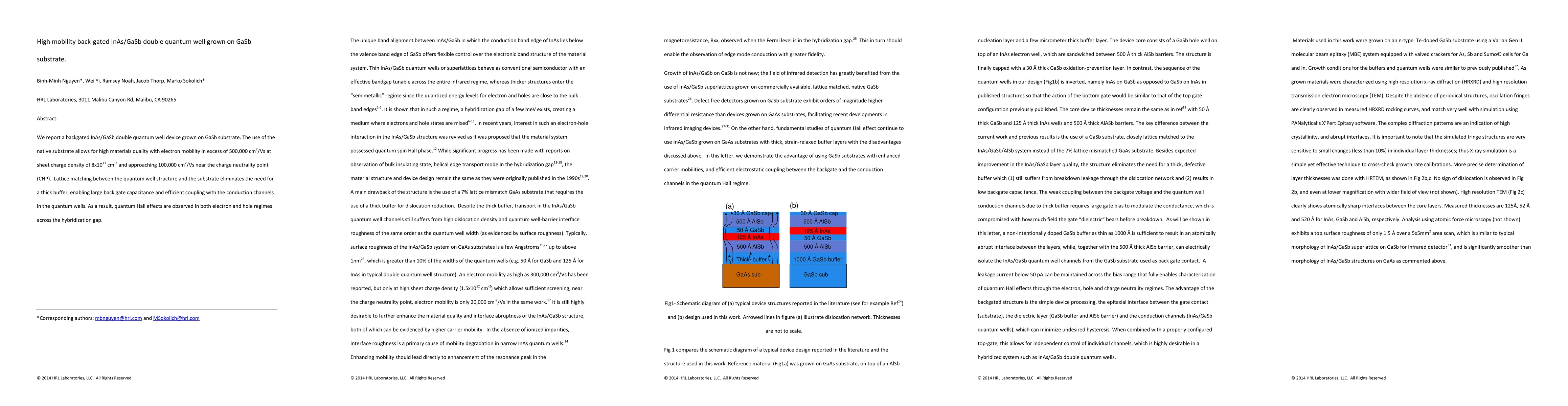
We report a backgated InAs/GaSb double quantum well device grown on GaSb substrate. The use of the native substrate allows for high materials quality with electron mobility in excess of 500,000 cm2/Vs at sheet charge density of 8x1011 cm-2 and approaching 100,000 cm2/Vs near the charge neutrality point (CNP). Lattice matching between the quantum well structure and the substrate eliminates the need for a thick buffer, enabling large back gate capacitance and efficient coupling with the conduction channels in the quantum wells. As a result, quantum Hall effects are observed in both electron and hole regimes across the hybridization gap.

Citation & Reference Network Visualization

This graph shows how this paper is connected to other research. The current paper is shown in dark gray, papers that cite it are in green, and papers it references are in blue. You can:

Current Paper
Papers citing this work (Citations)
Papers cited by this work (References)

• Hover over any node to see the paper title

• Click a node to view that paper's details

• Drag nodes to rearrange the graph

• Use the zoom controls (bottom right) to zoom in/out

Citations and References

Title Authors Year Actions
Structural design and molecular beam epitaxy growth of GaAs and InAs heterostructures for high mobility two-dimensional electron gas
Tiantian Wang, Huading Song, Ke He
2024
View Paper
Magnetocapacitance oscillations dominated by giant Rashba spin orbit interaction in InAs/GaSb quantum wells separated by AlSb barrier
A.S.L. Ribeiro, R. Schott, C. Reichl, W. Dietsche, W. Wegscheider
2024
View Paper
Coexistence of topological and normal insulating phases in electro-optically tuned InAs/GaSb bilayer quantum wells
M. Meyer, Tobias Fahndrich, Sebastian Schmid, Adriana Wolf, S. Krishtopenko, Benoit Jouault, G. Bastard, F. Teppe, F. Hartmann, S. Hofling
2024
View Paper
Topological band structure in InAs/GaSb/InAs triple quantum wells
M. Meyer, S. Schmid, F. Jabeen, G. Bastard, F. Hartmann, S. Höfling
2021
View Paper
Scattering in InAs/GaSb coupled quantum wells as a probe of higher order subband hybridization
C. S. Knox, Lianhe H. Li, M. Rosamond, E. Linfield, C. Marrows
2020
View Paper
Impact of epitaxial strain on the topological-nontopological phase diagram and semimetallic behavior of InAs/GaSb composite quantum wells
H. Irie, T. Akiho, F. Couedo, Ruben Ohana, K. Suzuki, K. Onomitsu, K. Muraki
2020
View Paper
Band Structure of InAs/GaSb coupled quantum wells studied by magnetotransport
C. S. Knox
2019
View Paper
Superconducting quantum interference in semiconducting Josephson junctions
de Vries
2019
View Paper
Deconvolution of Rashba and Dresselhaus spin-orbit coupling by crystal axis dependent measurements of coupled InAs/GaSb quantum wells
C. S. Knox, Lianhe H. Li, M. Rosamond, E. Linfield, C. Marrows
2018
View Paper
Optical tuning of the charge carrier type in the topological regime of InAs/GaSb quantum wells
G. Knebl, P. Pfeffer, S. Schmid, M. Kamp, G. Bastard, E. Batke, L. Worschech, F. Hartmann, S. Höfling
2018
View Paper
Low-temperature conductivity of weakly interacting quantum spin Hall edges in strained-layer InAs/GaInSb
Tingxin Li, Pengjie Wang, G. Sullivan, Xi Lin, R. Du
2017
View Paper
Circular and linear photogalvanic effects in type-II GaSb/InAs quantum well structures in the inverted regime
H. Plank, S. Tarasenko, T. Hummel, G. Knebl, P. Pfeffer, M. Kamp, S. Höfling, S. Höfling, S. Ganichev
2016
View Paper
Mobility enhancement of strained GaSb p-channel metal-oxide-semiconductor field-effect transistors with biaxial compressive strain
Yanwen Chen, Z. Tan, Lianfeng Zhao, Jing Wang, Yizhou Liu, Chen Si, Fang-Yuan Yuan, W. Duan, Jun Xu
2016
View Paper
Edge transport in the trivial phase of InAs/GaSb
F. Nichele, H. Suominen, M. Kjaergaard, C. Marcus, Ebrahim Sajadi, J. Folk, F. Qu, A. Beukman, Folkert Vries, J. V. Veen, S. Nadj-Perge, L. Kouwenhoven, B. Nguyen, A. Kiselev, W. Yi, M. Sokolich, M. Manfra, E. Spanton, K. Moler
2015
View Paper
Deconvolution of Rashba and Dresselhaus spin orbit coupling by crystal axis dependent measurements in InAs/GaSb coupled quantum wells
S. Knox, L. Li, M. Rosamond, E. Linfield, C. Marrows
2018
View Paper
Epitaxial interfaces between superconductors and semiconductors
P. Krogstrup, N. Ziino, W. Chang, S. Albrecht, M. Madsen, E. Johnson, J. Nygård, C. Marcus, T. Jespersen, F. Kuemmeth
2015
View Paper

Comments (0)

This website uses cookies to ensure you get the best experience. Learn more