Summary
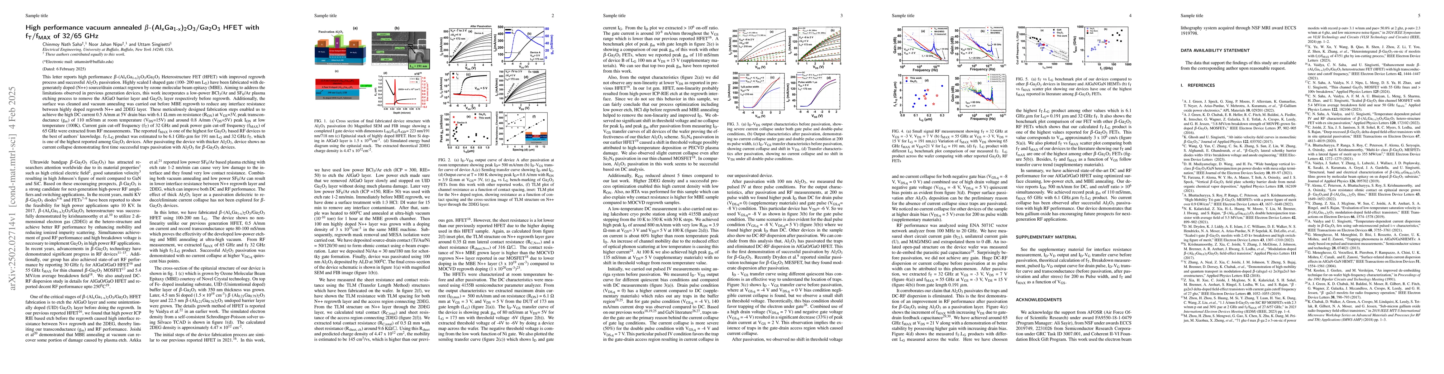
This letter reports high performance beta-(AlxGa1-x)2O3/Ga2O3 Heterostructure FET (HFET) with improved regrowth process. Highly scaled I shaped gate have been fabricated with degenerately doped (N++) source/drain contact regrown by ozone molecular beam epitaxy (MBE). Aiming to address the limitations observed in previous generation devices, this work incorporates a low-power BCl3/Ar and SF6/Ar plasma etching process to remove the AlGaO barrier layer and Ga2O3 layer respectively before regrowth. Additionally, the surface was cleaned and vacuum annealing was carried out before MBE regrowth to reduce any interface resistance between highly doped regrowth N++ and 2DEG layer. These meticulously designed fabrication steps enabled us to achieve the high DC current 0.5 A/mm at 5V drain bias with 6.1 $\mathrm{\Omega}$.mm on resistance (R\textsubscript{ON}) at V_GS=3V, peak transconductance (g_m) of 110 mS/mm at room temperature (V_DS=15V) and around 0.8 A/mm (V_DS=5V) peak I_ON} at low temperature (100K). Current gain cut-off frequency (f_T) of 32 GHz and peak power gain cut-off frequency (f_MAX) of 65 GHz were extracted from RF measurements. f_T.L_G product was estimated to be 6.1 GHz-$\mu$m for 191 nm L_G and 32 GHz f_T, which is one of the highest reported among Ga2O3 devices. With thicker Al2O3, device shows no current collapse demonstrating first time successful traps passivation with Al2O3 for Ga2O3 devices.
AI Key Findings
Generated Jun 12, 2025
Methodology
The research utilizes an improved regrowth process for beta-(AlxGa1-x)2O3/Ga2O3 Heterostructure FET (HFET), incorporating low-power BCl3/Ar and SF6/Ar plasma etching, surface treatment, and vacuum annealing before MBE regrowth.
Key Results
- Achieved high DC current of 0.5 A/mm at 5V drain bias with 6.1 $\mathrm{\Omega}$.mm on resistance (R_ON) at V_GS=3V.
- Obtained peak transconductance (g_m) of 110 mS/mm at room temperature (V_DS=15V) and around 0.8 A/mm (V_DS=5V) peak I_ON at low temperature (100K).
- Extracted current gain cut-off frequency (f_T) of 32 GHz and peak power gain cut-off frequency (f_MAX) of 65 GHz from RF measurements.
- Estimated f_T.L_G product to be 6.1 GHz-$\mu$m for 191 nm L_G and 32 GHz f_T.
- Demonstrated successful traps passivation with Al2O3 for Ga2O3 devices, showing no current collapse with thicker Al2O3.
Significance
This work presents high-performance Ga2O3 HFETs with improved fabrication steps, achieving high DC current, low on-resistance, and excellent RF characteristics, highlighting Ga2O3's potential for next-generation RF applications.
Technical Contribution
The paper introduces an optimized fabrication process for Ga2O3 HFETs, including low-power plasma etching, surface treatment, and vacuum annealing, leading to improved device performance.
Novelty
This research presents a novel approach to enhancing Ga2O3 HFET performance through meticulously designed fabrication steps, achieving high DC current, low on-resistance, and excellent RF characteristics, which sets it apart from previous works on Ga2O3 devices.
Limitations
- The research did not investigate the long-term stability of the devices.
- The study did not compare the performance with other wide-bandgap semiconductors like GaN or SiC.
Future Work
- Investigate the long-term reliability and stability of these devices under various operating conditions.
- Compare the performance of Ga2O3 HFETs with other wide-bandgap semiconductor technologies for potential applications.
Paper Details
PDF Preview
Similar Papers
Found 4 papersMetalorganic Chemical Vapor Deposition of \b{eta}-(AlxGa1-x)2O3 thin films on (001) \b{eta}-Ga2O3 substrates
Chris Chae, Jinwoo Hwang, Lingyu Meng et al.
No citations found for this paper.
Comments (0)