Publication
Metrics
AI Quick Summary
This paper reports the first successful growth of high-quality, atomically thin PtSe2 films using molecular beam epitaxy, achieving layers from 1 to 22 monolayers and demonstrating their potential for high-speed electronics, spintronics, and photodetectors through comprehensive characterization and electronic structure analysis.
Paper Preview
Abstract
Atomically thin PtSe2 films have attracted extensive research interests for potential applications in high-speed electronics, spintronics and photodetectors. Obtaining high quality, single crystalline thin films with large size is critical. Here we report the first successful layer-by-layer growth of high quality PtSe2 films by molecular beam epitaxy. Atomically thin films from 1 ML to 22 ML have been grown and characterized by low-energy electron diffraction, Raman spectroscopy and X-ray photoemission spectroscopy. Moreover, a systematic thickness dependent study of the electronic structure is revealed by angle-resolved photoemission spectroscopy (ARPES), and helical spin texture is revealed by spin-ARPES. Our work provides new opportunities for growing large size single crystalline films for investigating the physical properties and potential applications of PtSe2.
AI Key Findings
Get AI-generated insights about this paper's methodology, results, significance, and more — seven facets brought into focus.
Impact
Paper Details
PDF Preview
Key Terms
Citation Network
Current paper (gray), citations (green), references (blue)
Display is limited for performance on very large graphs.
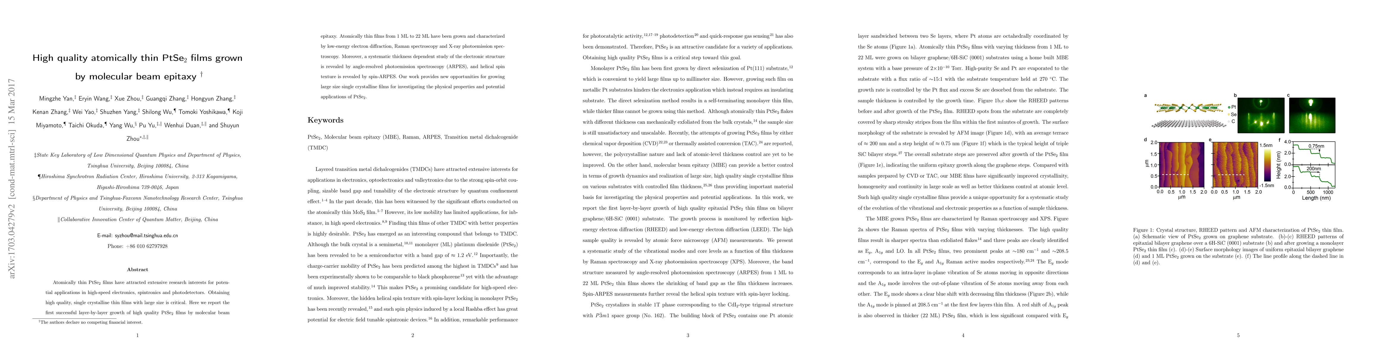
Discussion 0