This study uses high-resolution cathodoluminescence hyperspectral imaging to analyze InGaN/GaN multiple quantum wells (MQWs), revealing that trench-like features exhibit red-shifted and more intense emission, while V-pits show blue-shifted and weaker emission, providing insights into nanoscale variations in MQW structures.
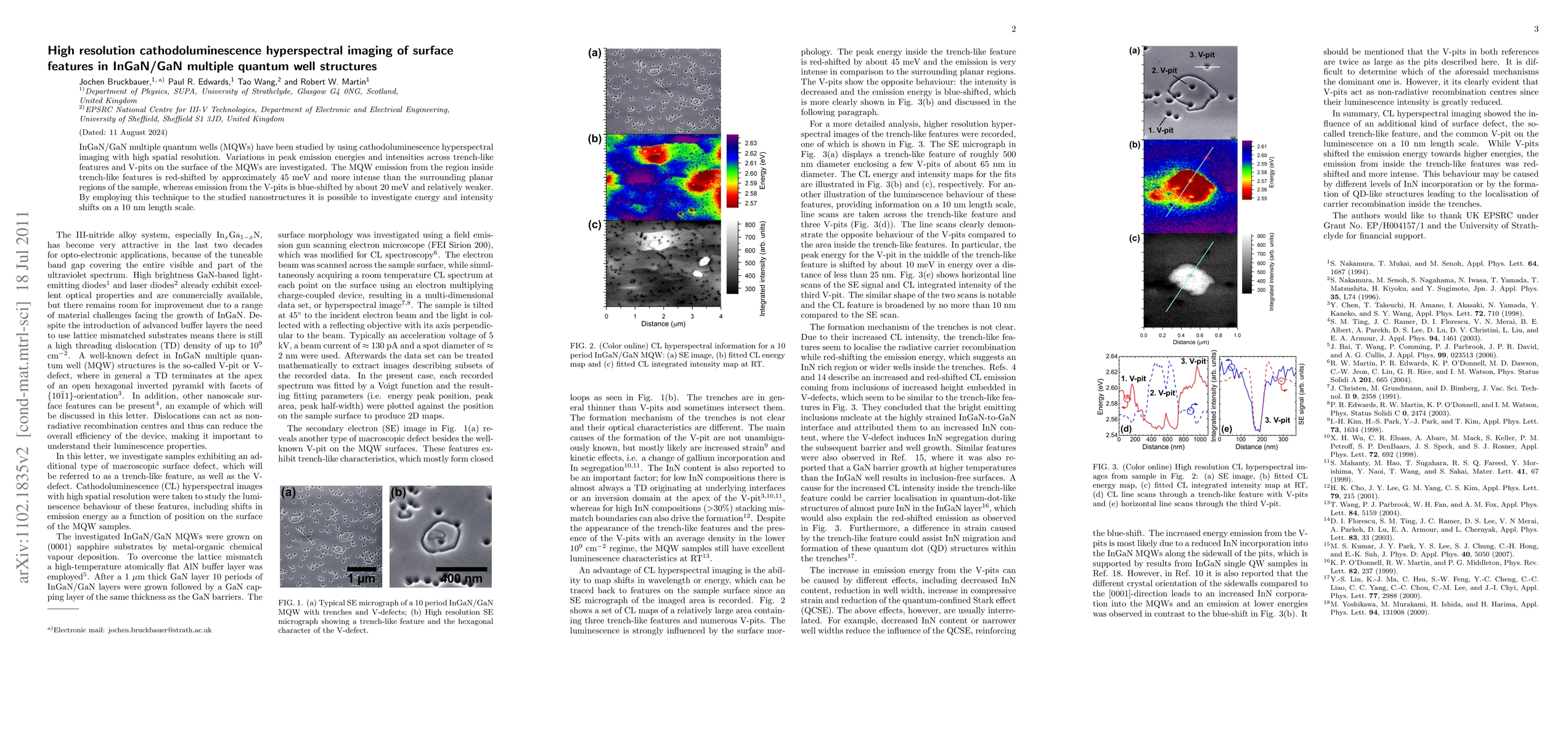
InGaN/GaN multiple quantum wells (MQWs) have been studied by using cathodoluminescence hyperspectral imaging with high spatial resolution. Variations in peak emission energies and intensities across trench-like features and V-pits on the surface of the MQWs are investigated. The MQW emission from the region inside trench-like features is red-shifted by approximately 45 meV and more intense than the surrounding planar regions of the sample, whereas emission from the V-pits is blue-shifted by about 20 meV and relatively weaker. By employing this technique to the studied nanostructures it is possible to investigate energy and intensity shifts on a 10 nm length scale.
Get AI-generated insights about this paper's methodology, results, and significance.
Current paper (gray), citations (green), references (blue)
Title | Authors | Year | Actions |
---|---|---|---|
Properties of V-defect injectors in long wavelength GaN LEDs studied by near-field electro- and photoluminescence
|
Rinat Yapparov, T. Tak, Jake Ewing, Shuji Nakamura, S. Denbaars, J. Speck, S. Marcinkevičius
|
2024
|
View Paper |
V-Pits and Trench-Like Defects in High Periodicity MQWs GaN-Based Solar Cells: Extensive Electro-Optical Analysis
|
M. Nicoletto, A. Caria, F. Rampazzo, C. de Santi, M. Buffolo, F. Rossi, Xuanqui Huang, H. Fu, H. Chen, Yuji Zhao, Andrea Gasparotto, Conny Becht, U. T. Schwarz, G. Meneghesso, E. Zanoni, M. Meneghini
|
2024
|
View Paper |
Mechanism of V-Shaped Pits on Promoting Hole Injection in the InGaN MQWs: First-Principles Investigation
|
Qingqing Feng, Li Liu, Yu Zhang, Xiaolu Zhu, Hai Kuang, Mingbin Zhou, Juanli Zhao, Ning Wu, Zhihua Xiong
|
2024
|
View Paper |
Efficient InGaN‐Based Red Light‐Emitting Diodes by Modulating Trench Defects
|
Z. Pan, Z. Chen, H. Zhang, H. Yang, Y. Chen, J. Nie, C. Deng, B. Dong, D. Wang, Y. Li, H. Lin, W. Chen, F. Jiao, X. Kang, C. Jia, Zhaohui Liang, Q. Wang, G. Zhang, B. Shen
|
2023
|
View Paper |
CL as a tool for device characterisation: the case of laser diode degradation
|
S. Dadgostar, J. Souto, J. Jiménez
|
2021
|
View Paper |
Improving the homogeneity and quality of InGaN/GaN quantum well exhibiting high In content under low TMIn flow and high pressure growth
|
Xiaowei Wang, F. Liang, Degang Zhao, Zongshun Liu, Jian-jun Zhu, Liyuan Peng, Jing Yang
|
2021
|
View Paper |
Influence of micro-patterning of the growth template on defect reduction and optical properties of non-polar (112ˉ0) GaN
|
J. Bruckbauer, Y. Gong, L. Jiu, M. J. Wallace, Anja Ipsen, S. Bauer, R. Müller, J. Bai, K. Thonke, Tao Wang, C. Trager-Cowan, R. Martin
|
2020
|
View Paper |
Influence of an InGaN superlattice pre-layer on the performance of semi-polar (11–22) green LEDs grown on silicon
|
X. Zhao, K. Huang, J. Bruckbauer, S. Shen, C. Zhu, P. Fletcher, P. Feng, Y. Cai, J. Bai, C. Trager-Cowan, R. Martin, T. Wang
|
2020
|
View Paper |
Mechanism of trench defect formation in InGaN/GaN single quantum well grown on single-crystal GaN substrate
|
Takashi Tange, Taeko Matsukata, T. Sannomiya
|
2020
|
View Paper |
Structural and luminescence imaging and characterisation of semiconductors in the scanning electron microscope
|
C. Trager-Cowan, A. Alasmari, W. Avis, J. Bruckbauer, Paul R. Edwards, Gergely Ferenczi, B. Hourahine, A. Kotzai, S. Kraeusel, G. Kusch, Robert W. Martin, R. McDermott, G. Naresh-Kumar, M. Nouf-Allehiani, E. Pascal, D. Thomson, S. Vespucci, M. D. Smith, P. Parbrook, J. Enslin, F. Mehnke, C. Kuhn, T. Wernicke, M. Kneissl, S. Hagedorn, A. Knauer, S. Walde, M. Weyers, P. Coulon, P. Shields, J. Bai, Y. Gong, L. Jiu, Yonghao Zhang, R. Smith, Tao Wang, Aimo Winkelmann
|
2020
|
View Paper |
Luminescence behavior of semipolar ( 10 1 ¯ 1 ) InGaN/GaN “bow-tie” structures on patterned Si substrates
|
J. Bruckbauer, C. Trager-Cowan, B. Hourahine, A. Winkelmann, P. Vennégués, Anja Ipsen, Xiang Yu, Xunming Zhao, M. J. Wallace, P. Edwards, G. Naresh-Kumar, M. Hocker, S. Bauer, R. Müller, J. Bai, K. Thonke, Tao Wang, R. Martin
|
2020
|
View Paper |
Effects of indium flow rate on the structural, morphological, optical and electrical properties of InGaN layers grown by metal organic chemical vapour deposition
|
K. Prabakaran, R. Ramesh, P. Arivazhagan, M. Jayasakthi, S. Sanjay, S. Surender, S. Pradeep, M. Balaji, K. Baskar
|
2019
|
View Paper |
Reduction of nonradiative recombination in InGaN epilayers grown with periodical dilute hydrogen carrier gas
|
Hailong Wang, Zesheng Lv, Chong Chen, Supeng Zhang, Yao Guo, Bin Li, Zhisheng Wu, Hao Jiang
|
2019
|
View Paper |
Scanning electron microscopy as a flexible technique for investigating the properties of UV-emitting nitride semiconductor thin films
|
C. Trager-Cowan, A. Alasmari, W. Avis, J. Bruckbauer, P. Edwards, B. Hourahine, S. Kraeusel, G. Kusch, R. Johnston, G. Naresh-Kumar, R. Martin, M. Nouf-Allehiani, E. Pascal, Lucia Spasevski, D. Thomson, S. Vespucci, P. Parbrook, M. D. Smith, J. Enslin, F. Mehnke, M. Kneissl, C. Kuhn, T. Wernicke, S. Hagedorn, A. Knauer, V. Kueller, S. Walde, M. Weyers, P. Coulon, P. Shields, Yonghao Zhang, L. Jiu, Y. Gong, R. Smith, Tao Wang, A. Winkelmann
|
2019
|
View Paper |
Microscopy of defects in semiconductors
|
F. Massabuau, J. Bruckbauer, C. Trager-Cowan, R. Oliver
|
2019
|
View Paper |
Preventing trench defect formation in InGaN epilayers using Ga-migration-enhanced epitaxy
|
Hailong Wang, Zesheng Lv, Supeng Zhang, Bin Li, Zhisheng Wu, Hao Jiang
|
2019
|
View Paper |
Influence of InN and AlN concentration on the compositional inhomogeneity and formation of InN-rich regions in InxAlyGa1−x−yN
|
G. Kusch, J. Enslin, Lucia Spasevski, Tolga Teke, T. Wernicke, P. Edwards, M. Kneissl, R. Martin
|
2019
|
View Paper |
Determining GaN Nanowire Polarity and its Influence on Light Emission in the Scanning Electron Microscope.
|
G. Naresh-Kumar, J. Bruckbauer, A. Winkelmann, Xiang Yu, B. Hourahine, P. Edwards, Tao Wang, C. Trager-Cowan, R. Martin
|
2019
|
View Paper |
Monolithic multiple colour emission from InGaN grown on patterned non-polar GaN
|
Y. Gong, L. Jiu, J. Bruckbauer, J. Bai, R. Martin, T. Wang
|
2019
|
View Paper |
Correlation between pit formation and phase separation in thick InGaN film on a Si substrate
|
H. Woo, Y. Jo, Jongmin Kim, Sangeun Cho, C. Roh, J. H. Lee, Hyungsang Kim, C. Hahn, H. Im
|
2018
|
View Paper |
GaN/AlGaN multiple quantum wells grown on transparent and conductive (-201)-oriented β-Ga2O3 substrate for UV vertical light emitting devices
|
I. Ajia, Y. Yamashita, Katharina Lorenz, M. Muhammed, Lucia Spasevski, D. Almalawi, J. Xu, K. Iizuka, Y. Morishima, D. Anjum, Nini Wei, Robert W. Martin, A. Kuramata, I. Roqan
|
2018
|
View Paper |
Probing the Local Electrical Properties of Al(In,Ga)N by Kelvin Probe Force Microscopy
|
A. Minj, H. B. Ammar, A. Cros, N. Garro, P. Gamarra, S. L. Delage, P. Ruterana
|
2018
|
View Paper |
Cathodoluminescence studies of chevron features in semi-polar (11-22) InGaN/GaN multiple quantum well structures
|
Catherine G. Brasser, J. Bruckbauer, Y. Gong, L. Jiu, J. Bai, M. Warzecha, P. Edwards, Tao Wang, R. Martin
|
2018
|
View Paper |
Effects of 4° misoriented sapphire substrate on optical property of green InGaN/GaN multiple quantum wells
|
R. Peng, J. Bai, Shengrui Xu, Jincheng Zhang, Jinjuan Du, Ying Zhao, Xiaomeng Fan, Mei Wu, Y. Hao
|
2017
|
View Paper |
Quantum well engineering in InGaN/GaN core-shell nanorod structures
|
Cg Bryce, E. Boulbar, P. Coulon, P. Edwards, I. Gîrgel, D. Allsopp, P. Shields, Robert W. Martin
|
2017
|
View Paper |
Spatially-resolved optical and structural properties of semi-polar \documentclass[12pt]{minimal} \usepackage{amsmath} \usepackage{wasysym} \usepackage{amsfonts} \usepackage{amssymb} \usepackage{amsbsy} \usepackage{mathrsfs} \usepackage{upgreek} \setlength{\oddsidemargin}{-69pt} \begin{document}$$\ma
|
J. Bruckbauer, Zhi Q. Li, G. Naresh-Kumar, M. Warzecha, P. Edwards, L. Jiu, Y. Gong, J. Bai, Tao Wang, C. Trager-Cowan, R. Martin
|
2017
|
View Paper |
Spatially-resolved optical and structural properties of semi-polar $$\mathrm{(11}\bar{2}\mathrm{2)}$$(112¯2) AlxGa1−xN with x up to 0.56
|
J. Bruckbauer, Zhi Q. Li, G. Naresh-Kumar, M. Warzecha, P. Edwards, L. Jiu, Y. Gong, J. Bai, Tao Wang, C. Trager-Cowan, R. Martin
|
2017
|
View Paper |
Nanoparticle discrimination based on wavelength and lifetime-multiplexed cathodoluminescence microscopy.
|
Mathijs W H Weppelman, I. Gerward, C. D. Boer, Pascal Martínez, Felipe Perona, Mathijs W. H. Garming, I. Weppelman, P. Boer, F. P. Martinez, R. Schirhagl, R. Moerland
|
2017
|
View Paper |
Carrier localization in the vicinity of dislocations in InGaN
|
F. Massabuau, Peiyu Chen, Matthew K. Horton, S. Rhode, C. Ren, T. O’Hanlon, A. Kovács, M. Kappers, C. Humphreys, R. Dunin‐Borkowski, R. Oliver
|
2017
|
View Paper |
Reprint of: Electron channelling contrast imaging for III-nitride thin film structures
|
G. Naresh-Kumar, D. Thomson, M. Nouf-Allehiani, J. Bruckbauer, P. Edwards, B. Hourahine, R. Martin, C. Trager-Cowan
|
2016
|
View Paper |
Influence of metalorganic precursors flow interruption timing on green InGaN multiple quantum wells
|
M. Dmukauskas, A. Kadys, T. Malinauskas, T. Grinys, I. Reklaitis, K. Badokas, M. Skapas, R. Tomašiūnas, D. Dobrovolskas, S. Stanionytė, I. Pietzonka, M. Strassburg, H. Lugauer
|
2016
|
View Paper |
Enhanced light output power of InGaN-based amber LEDs by strain-compensating AlN/AlGaN barriers
|
D. Iida, Shen Lu, Sota Hirahara, Kazumasa Niwa, S. Kamiyama, K. Ohkawa
|
2016
|
View Paper |
Electron channelling contrast imaging for III-nitride thin film structures
|
G. Naresh-Kumar, D. Thomson, M. Nouf-Allehiani, J. Bruckbauer, P. Edwards, B. Hourahine, R. Martin, C. Trager-Cowan
|
2016
|
View Paper |
Significant improvements in InGaN/GaN nano-photoelectrodes for hydrogen generation by structure and polarization optimization
|
T. Tao, Ting Zhi, Bin Liu, Ming-xue Li, Zhe Zhuang, J. Dai, Yi Li, Fulong Jiang, Wenjun Luo, Z. Xie, Dunjun Chen, Peng Chen, Zhaosheng Li, Z. Zou, Rong Zhang, Youdou Zheng
|
2016
|
View Paper |
Optimized In composition and quantum well thickness for yellow-emitting (Ga,In)N/GaN multiple quantum wells
|
K. Lekhal, Sakhawat Hussain, Sakhawat Hussain, P. Mierry, P. Vennégués, M. Nemoz, J. Chauveau, J. Chauveau, B. Damilano
|
2016
|
View Paper |
V-pits as Barriers to Diffusion of Carriers in InGaN/GaN Quantum Wells
|
M. Sheen, Sungdug Kim, Jong-Hwan Lee, J. Shim, Young-Woon Kim
|
2015
|
View Paper |
Temperature dependence of photoluminescence spectra for green light emission from InGaN/GaN multiple wells.
|
W. Liu, D. G. Zhao, D. Jiang, P. Chen, Z. Liu, J. Zhu, M. Shi, D. Zhao, X. Li, J. P. Liu, S. Zhang, H. Wang, H. Yang, Y. T. Zhang, G. Du
|
2015
|
View Paper |
Low-Temperature Cathodoluminescence Investigations of High-Quality Zinc Oxide Nanorods
|
B. Witkowski, L. Wachnicki, S. Gierałtowska, A. Reszka, B. Kowalski, M. Godlewski
|
2015
|
View Paper |
Effect of the barrier growth mode on the luminescence and conductivity micron scale uniformity of InGaN light emitting diodes
|
M. J. Wallace, P. Edwards, M. Kappers, M. Hopkins, F. Oehler, S. Sivaraya, R. Oliver, C. Humphreys, D. Allsopp, R. Martin
|
2015
|
View Paper |
Role of compositional fluctuations and their suppression on the strain and luminescence of InGaN alloys
|
K. Pantzas, G. Patriarche, D. Troadec, M. Kociak, N. Cherkashin, M. Hÿtch, J. Barjon, C. Tanguy, T. Rivera, S. Suresh, A. Ougazzaden
|
2015
|
View Paper |
Influence of stress on optical transitions in GaN nanorods containing a single InGaN/GaN quantum disk
|
Y. Zhuang, J. Bruckbauer, P. Shields, P. Edwards, R. Martin, D. Allsopp
|
2014
|
View Paper |
The impact of trench defects in InGaN/GaN light emitting diodes and implications for the ?green gap? problem
|
F. Massabuau, M. J. Davies, F. Oehler, S. Pamenter, E. Thrush, M. Kappers, A. Kovács, T. Williams, M. Hopkins, C. Humphreys, P. Dawson, R. Dunin‐Borkowski, J. Etheridge, D. Allsopp, R. Oliver
|
2014
|
View Paper |
Enhancement in solar hydrogen generation efficiency using InGaN photoelectrode after surface roughening treatment with nano-sized Ni mask
|
T. Tao, Zhi Ting, Liu Ming-xue, Xie Zili, Zhang Rong, Liu Bin, Li Yi, Zhuang Zhe, Zhang Guo-gang, Jiang Fulong, Chen Peng, Zheng You-dou
|
2014
|
View Paper |
Bias dependence and correlation of the cathodoluminescence and electron beam induced current from an InGaN/GaN light emitting diode
|
M. J. Wallace, P. Edwards, M. Kappers, M. Hopkins, F. Oehler, S. Sivaraya, D. Allsopp, R. Oliver, C. Humphreys, R. Martin
|
2014
|
View Paper |
Influence of quantum-confined Stark effect on optical properties within trench defects in InGaN quantum wells with different indium content
|
A. Vaitkevičius, J. Mickevičius, D. Dobrovolskas, Ö. Tuna, C. Giesen, M. Heuken, G. Tamulaitis
|
2014
|
View Paper |
Influence of V-pits on the efficiency droop in InGaN/GaN quantum wells.
|
Jaekyun Kim, Yong-Hee Cho, D. Ko, Xiang-Shu Li, J. Won, Eunha Lee, Seoung-Hwan Park, Junyoun Kim, Sungjin Kim
|
2014
|
View Paper |
Time resolved microscopic cathodoluminescence spectroscopy for phosphor research
|
D. Poelman, P. Smet
|
2014
|
View Paper |
The impact of growth parameters on trench defects in InGaN/GaN quantum wells
|
F. Massabuau, A. L. Fol, S. Pamenter, F. Oehler, M. Kappers, C. Humphreys, R. Oliver
|
2014
|
View Paper |
Effect of Secondary Electroluminescence on Cathodoluminescence and Other Luminescence Measurements
|
M. Pluska, A. Czerwiński, A. Szerling, J. Ratajczak, J. Kątcki
|
2014
|
View Paper |
Influence of barrier growth schemes on the structural properties and thresholds of InGaN quantum well laser diodes
|
V. Hoffmann, A. Mogilatenko, C. Netzel, U. Zeimer, S. Einfeldt, M. Weyers, M. Kneissl
|
2014
|
View Paper |
Cathodoluminescence hyperspectral imaging of trench-like defects in InGaN/GaN quantum well structures
|
J. Bruckbauer, P. Edwards, S. Sahonta, F. Massabuau, M. Kappers, C. Humphreys, R. Oliver, R. Martin
|
2014
|
View Paper |
Nanoscale characterisation of semiconductors by cathodoluminescence
|
K. Thonke, I. Tischer, M. Hocker, M. Schirra, K. Fujan, M. Wiedenmann, R. Schneider, M. Frey, M. Feneberg
|
2014
|
View Paper |
Influence of a low-temperature capping on the crystalline structure and morphology of InGaN quantum dot structures
|
B. Krause, B. Miljević, T. Aschenbrenner, E. Piskorska-Hommel, C. Tessarek, M. Barchuk, G. Buth, R. D. Tchana, S. Figge, J. Gutowski, D. Hänschke, J. Kalden, T. Laurus, S. Lazarev, R. Magalhães-Paniago, K. Sebald, A. Wolska, D. Hommel, J. Falta, V. Holý, T. Baumbach
|
2014
|
View Paper |
Physical properties of indium nitride, impurities, and defects
|
S. Khludkov, I. Prudaev, O. Tolbanov
|
2014
|
View Paper |
Towards a better understanding of trench defects in InGaN/GaN quantum wells
|
F. Massabuau, L. Trinh-Xuan, D. Lodié, S. Sahonta, S. Rhode, E. Thrush, F. Oehler, M. Kappers, C. Humphreys, R. Oliver
|
2013
|
View Paper |
Coincident Electron Channeling and Cathodoluminescence Studies of Threading Dislocations in GaN
|
G. Naresh-Kumar, J. Bruckbauer, P. Edwards, S. Kraeusel, B. Hourahine, R. Martin, M. Kappers, M. Moram, Stephen Lovelock, R. Oliver, C. Humphreys, C. Trager-Cowan
|
2013
|
View Paper |
Étude et caractérisations par cathodoluminescence de couches minces d'InGaN pour le photovoltaïque
|
Youssef El Gmili
|
2013
|
View Paper |
Multilayered InGaN/GaN structure vs. single InGaN layer for solar cell applications: A comparative study
|
Y. E. Gmili, G. Orsal, K. Pantzas, T. Moudakir, S. Sundaram, G. Patriarche, J. Hester, A. Ahaitouf, J. Salvestrini, A. Ougazzaden
|
2013
|
View Paper |
Probing light emission from quantum wells within a single nanorod
|
J. Bruckbauer, P. Edwards, J. Bai, Tao Wang, R. Martin
|
2013
|
View Paper |
Characteristics of the surface microstructures in thick InGaN layers on GaN
|
Y. E. Gmili, G. Orsal, K. Pantzas, A. Ahaitouf, T. Moudakir, S. Gautier, G. Patriarche, D. Troadec, J. Salvestrini, A. Ougazzaden
|
2013
|
View Paper |
Composition and luminescence studies of InGaN epilayers grown at different hydrogen flow rates
|
E. Taylor, F. Fang, F. Oehler, P. Edwards, M. Kappers, K. Lorenz, E. Alves, C. McAleese, C. Humphreys, R. Martin
|
2013
|
View Paper |
Correlations between the morphology and emission properties of trench defects in InGaN/GaN quantum wells
|
F. Massabuau, L. Trinh-Xuan, D. Lodié, E. Thrush, Dandan Zhu, F. Oehler, T. Zhu, M. Kappers, C. Humphreys, R. Oliver
|
2013
|
View Paper |
Properties of trench defects in InGaN/GaN quantum well structures
|
S. Sahonta, M. Kappers, Dandan Zhu, Tim J. Puchtler, T. Zhu, S. E. Bennett, C. Humphreys, R. Oliver
|
2013
|
View Paper |
Origin of the redshift of the luminescence peak in InGaN light-emitting diodes exposed to Co-60 γ-ray irradiation
|
Yan Li, Xing-Wen Wang, S. M. He, Baoping Zhang, L. X. Sun, Y. D. Li, Q. Guo, Changqin Chen, Zhanghai Chen, W. Lu
|
2012
|
View Paper |
Investigation of electrical and optical properties in semiconductor structures via SEM techniques with high spatial resolution
|
Eugene B. Yakimov
|
2012
|
View Paper |
High-Resolution Cathodoluminescence Hyperspectral Imaging of Nitride Nanostructures
|
P. Edwards, L. K. Jagadamma, J. Bruckbauer, Chaowang Liu, P. Shields, D. Allsopp, Tao Wang, R. Martin
|
2012
|
View Paper |
Morphological, structural, and emission characterization of trench defects in InGaN/GaN quantum well structures
|
F. Massabuau, S. Sahonta, L. Trinh-Xuan, S. Rhode, Tim J. Puchtler, M. Kappers, C. Humphreys, R. Oliver
|
2012
|
View Paper |
Quantum-confined stark effect in localized luminescent centers within InGaN/GaN quantum-well based light emitting diodes
|
S. De, Arunasish Layek, Sukanya Bhattacharya, D. Das, A. Kadir, Arnab Bhattacharya, S. Dhar, Arindam Chowdhury
|
2012
|
View Paper |
Visualizing highly localized luminescence in GaN/AlN heterostructures in nanowires
|
L. Zagonel, L. Rigutti, M. Tchernycheva, G. Jacopin, R. Songmuang, M. Kociak
|
2012
|
View Paper |
Defect detection in semiconductor layers with built-in electric field with the use of cathodoluminescence
|
M. Pluska, A. Czerwiński, J. Ratajczak, A. Szerling, J. Kątcki
|
2012
|
View Paper |
Cathodoluminescence and Electroluminescence of Semiconductor Structures in SEM
|
M. Pluska, A. Czerwiński, J. Ratajczak, A. Szerling, J. Kątcki
|
2012
|
View Paper |
Optoelectronic behaviors and carrier dynamics of individual localized luminescent centers in InGaN quantum-well light emitting diodes
|
S. De, D. Das, Arunasish Layek, A. Raja, M. Singh, Arnab Bhattacharya, S. Dhar, Arindam Chowdhury
|
2011
|
View Paper |
Cathodoluminescence nano-characterization of semiconductors
|
P. Edwards, R. Martin
|
2011
|
View Paper |
multiple colour emission from InGaN grown on patterned non-polar
|
L. Jiu, J. Bruckbauer, J. Bai, R. Martin, T. Wang
|
2019
|
View Paper |
The scanning electron microscope as a flexible tool for investigating the properties of UV-emitting nitride semiconductor thin films
|
T. C., Rager, C. -, Owan, A. A., Lasmari, B. J., Ruckbauer, E. P.R., dwards, H. B., Ourahine, K. S., Raeusel, K. G, usch, J. R., Ohnston, N. G., Aresh, K. ., Umar, M. R.W., Artin, N. M., Ouf, A. –, Llehiani, P. E., Ascal, S. L., Pasevski, T. D., Homson, V. S., Espucci, P. P.J., Arbrook, Sergio Pecorelli M.D., mith, E. J., Nslin, M. F., Ehnke, K. M., Neissl, K. C., uhn, W. T., Ernicke, H. S., Agedorn, K. A., Nauer, K. V., Ueller, W. S., Alde, W. M., Eyers, C. P.-M., Oulon, S. P.-A., Hields, Z. Y., Hang, J. L., iu, G. Y., ong, S. R.M., Ang, W. A., Inkelmann
|
2019
|
View Paper |
Investigation of indium-rich InGaN alloys and kinetic growth regime of GaN
|
N. Kaufmann
|
2013
|
View Paper |
Cathodoluminescence hyperspectral imaging on the nanometre scale
|
P. Edwards, L. K. Jagadamma, R. Martin, A. Wark
|
2011
|
View Paper |
Comments (0)