The study employs scanning nitrogen-vacancy (NV) center electrometry with an axially symmetric probe that uses intermittent-contact mode to achieve high-resolution electric field imaging. The probe features sub-nanometer oscillating amplitude and provides robust feedback for maintaining close engagement with the sample.
High-resolution electric field imaging based on intermittent-contact mode scanning NV center electrometry
Publication
Metrics
Quick Answers
What methodology did the authors use?
The study employs scanning nitrogen-vacancy (NV) center electrometry with an axially symmetric probe that uses intermittent-contact mode to achieve high-resolution electric field imaging. The probe features sub-nanometer oscillating amplitude and provides robust feedback for maintaining close engagement with the sample. More in Methodology →
What are the key results?
Achieved a spatial resolution of approximately 10 nm — Demonstrated the ability to resolve nanoscale polar textures and dynamics in ferroelectric lithium niobate More in Key Results →
Why is this work significant?
This research enables direct observation of nanoscale electric field structures in ferroelectric materials, which is critical for understanding their polarization dynamics and could advance applications in nanoscale electronics and memory devices. More in Significance →
What are the main limitations?
Surface screening effects may smooth electric field profiles — Resolution is limited by the NV-sample distance and mechanical oscillation amplitude More in Limitations →
Abstract
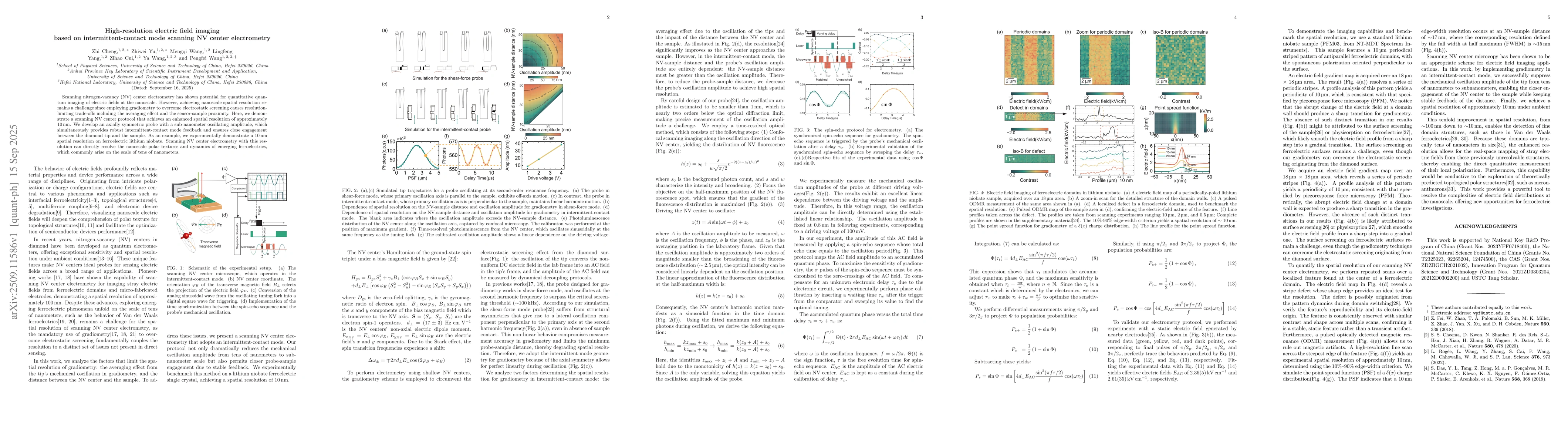
Scanning nitrogen-vacancy (NV) center electrometry has shown potential for quantitative quantum imaging of electric fields at the nanoscale. However, achieving nanoscale spatial resolution remains a challenge since employing gradiometry to overcome electrostatic screening causes resolution-limiting trade-offs including the averaging effect and the sensor-sample proximity. Here, we demonstrate a scanning NV center protocol that achieves an enhanced spatial resolution of approximately 10 nm. We develop an axially symmetric probe with a sub-nanometer oscillating amplitude, which simultaneously provides robust intermittent-contact mode feedback and ensures close engagement between the diamond tip and the sample. As an example, we experimentally demonstrate a 10 nm spatial resolution on ferroelectric lithium niobate. Scanning NV center electrometry with this resolution can directly resolve the nanoscale polar textures and dynamics of emerging ferroelectrics, which commonly arise on the scale of tens of nanometers.
Key Findings, in focus
Seven facets of this paper, analysed and brought into focus by AI.
This research enables direct observation of nanoscale electric field structures in ferroelectric materials, which is critical for understanding their polarization dynamics and could advance applications in nanoscale electronics and memory devices.
- Achieved a spatial resolution of approximately 10 nm
- Demonstrated the ability to resolve nanoscale polar textures and dynamics in ferroelectric lithium niobate
- Validated the method using electric field maps and line profiles showing consistent results
This research enables direct observation of nanoscale electric field structures in ferroelectric materials, which is critical for understanding their polarization dynamics and could advance applications in nanoscale electronics and memory devices.
Development of an intermittent-contact mode scanning NV center protocol with sub-nanometer oscillation amplitude for enhanced spatial resolution
Combines intermittent-contact mode with gradiometry to suppress mechanical oscillation amplitude, achieving sub-nanometer resolution in electric field imaging for the first time
- Surface screening effects may smooth electric field profiles
- Resolution is limited by the NV-sample distance and mechanical oscillation amplitude
- Exploring applications in other ferroelectric materials
- Improving resolution further by optimizing NV-sample distance and oscillation parameters
Discussion 0