This paper identifies over 100 anti-gap semiconductors using high-throughput computation, focusing on the MX$_2$ family (M=Hf, Zr; X=S, Se). These materials exhibit strong defect tolerance and unique photoinduced lattice dynamics, potentially enabling photo-driven thermal switches.
Conventional semiconductors typically have bonding states near the valence band maximum (VBM) and antibonding states near the conduction band minimum (CBM). Semiconductors with the opposite electronic configuration, namely an antibonding VBM and a bonding CBM, are here termed ``anti-gap semiconductors". They have been theoretically proposed to exhibit excellent optoelectronic properties because of their strong tolerance to defects. However, no anti-gap semiconductors have been identified so far, despite a known list of semiconductors with an antibonding VBM. Here, we use high-throughput computation to identify over 100 anti-gap semiconductors. From this group, we analyze the transition metal dichalcogenide MX$_2$ (M=Hf, Zr; X=S, Se) family in detail. In addition to verifying their defect tolerance for both electrons and holes using first-principles simulations, we also discovered that photoexcitation of charge carriers can lead to significant lattice stiffening and increased thermal conductivity in anti-gap semiconductors, which can be potentially used as photo-driven thermal switches. Our work analyzes the formation of the anti-gap electronic structure and showcases their unusual photoinduced lattice dynamics that can have a potential impact on their photophysical applications.
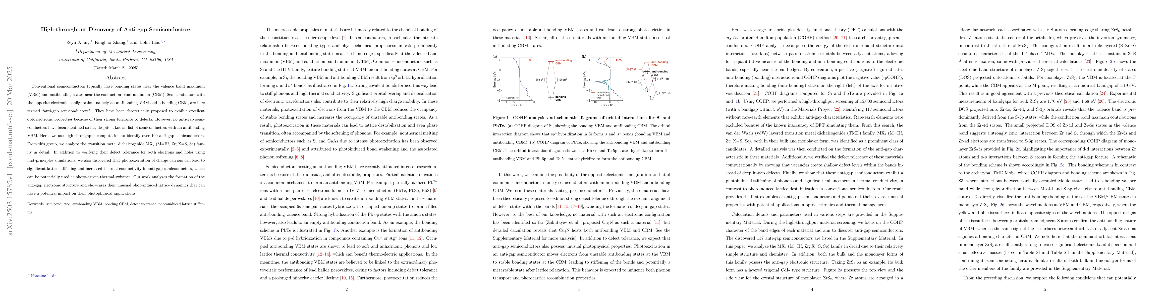
Generated Jun 10, 2025
The research utilized high-throughput density functional theory (DFT) calculations via the Vienna Ab initio Simulation Package (VASP) with the Perdew-Burke-Ernzerhof (PBE) form of the generalized gradient approximation (GGA). Crystal orbital Hamilton populations (COHP) analysis was performed using LOBSTER to decompose electronic band structure energies into atomic orbital interactions.
This work is significant as it identifies anti-gap semiconductors, theoretically proposed for their excellent optoelectronic properties due to strong defect tolerance, which were previously undiscovered despite known lists of semiconductors with an antibonding valence band maximum.
The paper presents a high-throughput computational method for discovering anti-gap semiconductors, utilizing DFT and COHP analysis to identify and characterize these materials.
The novelty of this research lies in its systematic identification of anti-gap semiconductors, a theoretical concept previously unrealized, and the discovery of their unusual photoinduced lattice dynamics.
Current paper (gray), citations (green), references (blue)
Display is limited for performance on very large graphs.
Andrea Crovetto, Mark Kamper Svendsen, Jiban Kangsabanik et al.
Hiroshi Mizuseki, Wen-Tong Geng, Gang Tang et al.
Weiwei Xie, Zhiqiang Mao, Venkatraman Gopalan et al.
Zhiqiang Xie, Jianchang Wu, Luca Torresi et al.
No citations found for this paper.
Comments (0)